SBAS221H December 2001 – October 2015 REG71050 , REG71055
PRODUCTION DATA.
- 1 Features
- 2 Applications
- 3 Description
- 4 Revision History
- 5 Device Comparison Table
- 6 Pin Configuration and Functions
- 7 Specifications
- 8 Detailed Description
- 9 Application and Implementation
- 10Power Supply Recommendations
- 11Layout
- 12Device and Documentation Support
- 13Mechanical, Packaging, and Orderable Information
Package Options
Mechanical Data (Package|Pins)
Thermal pad, mechanical data (Package|Pins)
- DRV|6
Orderable Information
1 Features
- Wide Input Voltage Range: 1.8 V to 5.5 V
- Automatic Step-Up and Step-Down Operation
- Low Input Current Ripple
- Low Output Voltage Ripple
- Minimum Number of External Components—No Inductors
- 1-MHz Internal Oscillator Allows Small Capacitors
- Shutdown Mode
- Thermal and Current Limit Protection
- Six Fixed Output Voltages Available:
2 Applications
- White LED Driver
- Smart Card Readers
- SIM Cards
- Handheld devices
- Modems
- PCMCIA Cards
- LCD Displays
- Battery Backup Supplies
3 Description
The REG710 family of devices are switched capacitor voltage converters that generate regulated, low-ripple output voltage from an unregulated input voltage. A wide input supply voltage from 1.8 V to 5.5 V makes the REG710 family of devices ideal for a variety of battery sources, such as single-cell Li-Ion, or 2-cell and 3-cell nickel-based or alkaline-based chemistries.
The input voltage may vary above and below the output voltage and the output remains in regulation. The device works as step-up or step-down converters without the need of an inductor, providing low EMI DC-DC conversion. The high switching frequency allows the use of small surface-mount capacitors, saving board space and reducing cost. The REG710 device is thermally protected and current limited, protecting the load and the regulator during fault conditions. Typical ground pin current (quiescent current) is 65 μA with no load, and less than 1 μA in shutdown mode.
Device Information(1)
| PART NUMBER | PACKAGE | BODY SIZE (NOM) |
|---|---|---|
| REG710 | SOT-23 (6) | 2.90 mm × 1.60 mm |
| REG71050 | SOT (6) | 2.90 mm × 1.60 mm |
| SON (6) | 2.00 mm × 2.00 mm | |
| REG71055 | SOT-23 (6) | 2.90 mm × 1.60 mm |
- For all available packages, see the orderable addendum at the end of the data sheet.
spacing
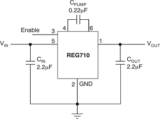
Typical Operating Circuit

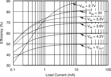
Efficiency vs Load Current
