SLVS577E March 2007 – December 2014 TPS61200 , TPS61201 , TPS61202
PRODUCTION DATA.
- 1 Features
- 2 Applications
- 3 Description
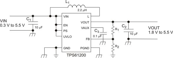
- 4 Typical Application
- 5 Revision History
- 6 Device Options
- 7 Pin Configuration and Functions
- 8 Specifications
- 9 Parameter Measurement Information
- 10Detailed Description
- 11Application and Implementation
- 12Power Supply Recommendations
- 13Layout
- 14Device and Documentation Support
- 15Mechanical, Packaging, and Orderable Information
Package Options
Mechanical Data (Package|Pins)
- DRC|10
Thermal pad, mechanical data (Package|Pins)
- DRC|10
Orderable Information
1 Features
- More than 90% Efficiency at
- Automatic Transition between Boost Mode and Down Conversion Mode
- Device Quiescent Current Less than 55 μA
- Startup into Full Load at 0.5 V Input Voltage
- Operating Input Voltage Range from
0.3 V to 5.5 V - Programmable Undervoltage Lockout Threshold
- Output Short Circuit Protection Under all Operating Conditions
- Fixed and Adjustable Output Voltage Options from 1.8 V to 5.5 V
- Power Save Mode for Improved Efficiency at Low Output Power
- Forced Fixed Frequency Operation Possible
- Load Disconnect During Shutdown
- Overtemperature Protection
- Small 3 mm x 3 mm VSON-10 Package
2 Applications
3 Description
The TPS6120x devices provide a power supply solution for products powered by either a single-cell, two-cell, or three-cell alkaline, NiCd or NiMH, or one-cell Li-Ion or Li-polymer battery. It is also used in fuel cell or solar cell powered devices where the capability of handling low input voltages is essential. Possible output currents depend on the input to output voltage ratio. The devices provide output currents of up to 600 mA at a 5-V output, while using a single-cell Li-Ion or Li-Polymer battery and discharges it down to 2.6 V. The boost converter is based on a fixed frequency, pulse-width-modulation (PWM) controller using synchronous rectification to obtain maximum efficiency. At low load currents, the converter enters the Power Save mode to maintain a high efficiency over a wide load current range. The Power Save mode can be disabled, forcing the converter to operate at a fixed switching frequency. The average input current is limited to a maximum value of 1500 mA. The output voltage is programmed by an external resistor divider, or is fixed internally on the chip. The converter can be disabled to minimize battery drain. During shutdown, the load is completely disconnected from the battery. The device is packaged in a 10-pin VSON package measuring 3 mm x 3 mm.
Device Information(1)
| PART NUMBER | PACKAGE | BODY SIZE (NOM) |
|---|---|---|
| TPS6120x | VSON (10) | 3.00 mm × 3.00 mm |
- For all available packages, see the orderable addendum at the end of the datasheet.
4 Typical Application