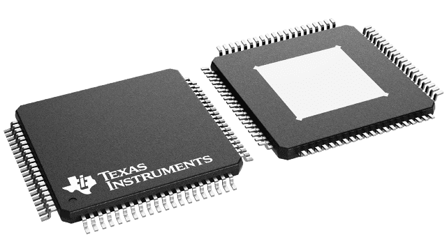
Packaging information
| Package | Pins HTQFP (PFP) | 80 |
| Operating temperature range (°C) -40 to 85 |
| Package qty | Carrier 1,000 | LARGE T&R |
Features for the ADS5281
- Speed and Resolution Grades:
- ADS5281: 12-bit, 50MSPS
- ADS5282: 12-bit, 65MSPS
- Power Dissipation:
- 48mW/Channel at 30MSPS
- 55mW/Channel at 40MSPS
- 64mW/Channel at 50MSPS
- 77mW/Channel at 65MSPS
- 70dBFS SNR at 10MHz IF
- Analog Input Full-Scale Range: 2VPP
- Low-Frequency Noise Suppression Mode
- 6dB Overload Recovery In One Clock
- External and Internal (Trimmed) Reference
- 3.3V Analog Supply, 1.8V Digital Supply
- Single-Ended or Differential Clock:
- Clock Duty Cycle Correction Circuit (DCC)
- Programmable Digital Gain: 0dB to 12dB
- Serialized DDR LVDS Output
- Programmable LVDS Current Drive, Internal Termination
- Test Patterns for Enabling Output Capture
- Straight Offset Binary or Two’s Complement Output
- Package Options:
- 9mm × 9mm QFN-64
- HTQFP-80 PowerPAD Compatible with ADS527x Family
Description for the ADS5281
The ADS528x is a family of high-performance, low-power, octal channel analog-to-digital converters (ADCs). Available in either a 9mm × 9mm QFN package or an HTQFP-80 package, with serialized low-voltage differential signaling (LVDS) outputs and a wide variety of programmable features, the ADS528x is highly customizable for a diversity of applications and offers an unprecedented level of system integration. An application note, XAPP774 (available at www.xilinx.com), describes how to interface the serial LVDS outputs of TI&3146;s ADCs to Xilinx field-programmable gate arrays (FPGAs). The ADS528x family is specified over the industrial temperature range of –40°C to +85°C.
