CD4541B

ACTIVO

Temporizador programable CMOS - Tipo de alta tensión (20 V nominales)

Detalles del producto

Technology family CD4000 Bits (#) 1 Rating Catalog Operating temperature range (°C) -55 to 125
PDIP (N) 14 181.42 mm² (19.3 mm × 9.4 mm) TSSOP (PW) 14 32 mm² (5 mm × 6.4 mm) SOIC (D) 14 51.9 mm² (8.65 mm × 6 mm) SOP (NS) 14 79.56 mm² (10.2 mm × 7.8 mm)
  • Low Symmetrical Output Resistance, Typically 100 at VDD = 15V
  • Built-In Low-Power RC Oscillator
  • Oscillator Frequency Range . . . DC to 100kHz
  • External Clock (Applied to Pin 3) can be Used Instead of Oscillator
  • Operates as 2 N Frequency Divider or as a Single-Transition Timer
  • Q/Q\ Select Provides Output Logic Level Flexibility
  • AUTO or MASTER RESET Disables Oscillator During Reset to Reduce Power Dissipation
  • Operates With Very Slow Clock Rise and Fall Times
  • Capable of Driving Six Low Power TTL Loads, Three Low-Power Schottky Loads, or Six HTL Loads Over the Rated Temperature Range
  • Symmetrical Output Characteristics
  • 100% Tested for Quiescent Current at 20V
  • 5V, 10V, and 15V Parametric Ratings
  • Meets All Requirements of JEDEC Standard No. 13B, "Standard Specifications for Description of ’B’ Series CMOS Devices"

Data sheet acquired from Harris Semiconductor

  • Low Symmetrical Output Resistance, Typically 100 at VDD = 15V
  • Built-In Low-Power RC Oscillator
  • Oscillator Frequency Range . . . DC to 100kHz
  • External Clock (Applied to Pin 3) can be Used Instead of Oscillator
  • Operates as 2 N Frequency Divider or as a Single-Transition Timer
  • Q/Q\ Select Provides Output Logic Level Flexibility
  • AUTO or MASTER RESET Disables Oscillator During Reset to Reduce Power Dissipation
  • Operates With Very Slow Clock Rise and Fall Times
  • Capable of Driving Six Low Power TTL Loads, Three Low-Power Schottky Loads, or Six HTL Loads Over the Rated Temperature Range
  • Symmetrical Output Characteristics
  • 100% Tested for Quiescent Current at 20V
  • 5V, 10V, and 15V Parametric Ratings
  • Meets All Requirements of JEDEC Standard No. 13B, "Standard Specifications for Description of ’B’ Series CMOS Devices"

Data sheet acquired from Harris Semiconductor

CD4541B programmable timer consists of a 16-stage binary counter, an oscillator that is controlled by external R-C components (2 resistors and a capacitor), an automatic power-on reset circuit, and output control logic. The counter increments on positive-edge clock transitions and can also be reset via the MASTER RESET input.

The output from this timer is the Q or Q\ output from the 8th, 10th, 13th, or 16th counter stage. The desired stage is chosen using time-select inputs A and B (see Frequency Select Table).

The output is available in either of two modes selectable via the MODE input, pin 10 (see Truth Table). When this MODE input is a logic "1", the output will be a continuous square wave having a frequency equal to the oscillator frequency divided by 2N. With the MODE input set to logic "0" and after a MASTER RESET is initiated, the output (assuming Q output has been selected) changes from a low to a high state after 2N-1 counts and remains in that state until another MASTER RESET pulse is applied or the MODE input is set to a logic "1".

Timing is initialized by setting the AUTO RESET input (pin 5) to logic "0" and turning power on. If pin 5 is set to logic "1", the AUTO RESET circuit is disabled and counting will not start until after a positive MASTER RESET pulse is applied and returns to a low level. The AUTO RESET consumes an appreciable amount of power and should not be used if low-power operation is desired. For reliable automatic power-on reset, VDD should be greater than 5V.

The RC oscillator, shown in Figure 2, oscillates with a frequency determined by the RC network and is calculated using:
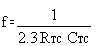
Where f is between 1kHz and 100kHz and RS and 2RTC.

CD4541B programmable timer consists of a 16-stage binary counter, an oscillator that is controlled by external R-C components (2 resistors and a capacitor), an automatic power-on reset circuit, and output control logic. The counter increments on positive-edge clock transitions and can also be reset via the MASTER RESET input.

The output from this timer is the Q or Q\ output from the 8th, 10th, 13th, or 16th counter stage. The desired stage is chosen using time-select inputs A and B (see Frequency Select Table).

The output is available in either of two modes selectable via the MODE input, pin 10 (see Truth Table). When this MODE input is a logic "1", the output will be a continuous square wave having a frequency equal to the oscillator frequency divided by 2N. With the MODE input set to logic "0" and after a MASTER RESET is initiated, the output (assuming Q output has been selected) changes from a low to a high state after 2N-1 counts and remains in that state until another MASTER RESET pulse is applied or the MODE input is set to a logic "1".

Timing is initialized by setting the AUTO RESET input (pin 5) to logic "0" and turning power on. If pin 5 is set to logic "1", the AUTO RESET circuit is disabled and counting will not start until after a positive MASTER RESET pulse is applied and returns to a low level. The AUTO RESET consumes an appreciable amount of power and should not be used if low-power operation is desired. For reliable automatic power-on reset, VDD should be greater than 5V.

The RC oscillator, shown in Figure 2, oscillates with a frequency determined by the RC network and is calculated using:

Where f is between 1kHz and 100kHz and RS and 2RTC.

Descargar Ver vídeo con transcripción Video

Productos similares que pueden interesarle

open-in-new Comparar alternativas
Funcionalidad similar a la del dispositivo comparado
TPL5010 ACTIVO Temporizador del sistema alimentado por nanopartículas con función de vigilancia y restablecimien Watchdog timer

Documentación técnica

No se encontraron resultados. Borre su búsqueda y vuelva a intentarlo.
Ver todo 1
Documentación principal Tipo Título Opciones de formato Descargar la versión más reciente en inglés Fecha
* Hoja de datos CD4541B datasheet (Rev. E) 21/08/2003

Diseño y desarrollo

Para conocer los términos adicionales o los recursos necesarios, haga clic en cualquier título de abajo para ver la página de detalles cuando esté disponible.

Placa de evaluación

14-24-LOGIC-EVM — Módulo de evaluación genérico de productos lógicos para encapsulados D, DB, DGV, DW, DYY, NS y PW de

El módulo de evaluación (EVM) 14-24-LOGIC-EVM está diseñado para admitir cualquier dispositivo lógico que se encuentre en un encapsulado D, DW, DB, NS, PW, DYY o DGV de 14 a 24 pines.

Guía del usuario: PDF | HTML
Productos y hardware compatibles
En inventario
Límite:
??asset.out-of-stock-ti_es_MX??
No disponible
Encapsulado Pines Símbolos CAD, huellas y modelos 3D
PDIP (N) 14 Ultra Librarian
TSSOP (PW) 14 Ultra Librarian
SOIC (D) 14 Ultra Librarian
SOP (NS) 14 Ultra Librarian

Pedidos y calidad

Soporte y capacitación

Foros de TI E2E™ con asistencia técnica de los ingenieros de TI

El contenido lo proporcionan “tal como está” TI y los colaboradores de la comunidad y no constituye especificaciones de TI. Consulte los términos de uso.

Si tiene alguna pregunta sobre calidad, encapsulados o pedido de productos de TI, consulte el servicio de asistencia de TI. ​​​​​​​​​​​​​​

Videos