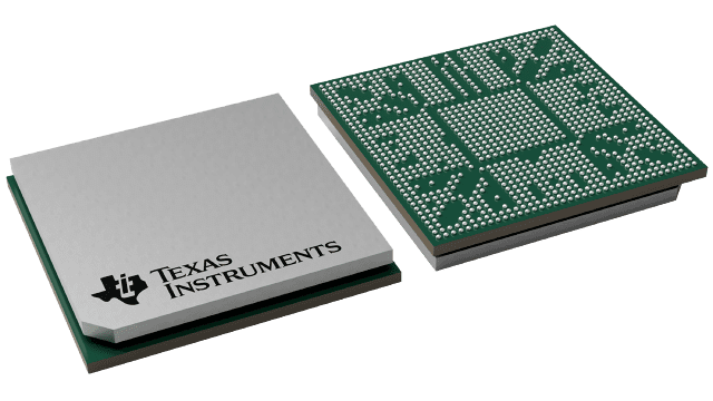
パッケージ情報
| パッケージ | ピン数 FCBGA (CYG) | 1031 |
| 動作温度範囲 (℃) 0 to 95 |
| パッケージ数量 | キャリア 44 | JEDEC TRAY (5+1) |
TMS320DM8168 の特徴
- High-Performance DaVinci Digital Media Processors
- ARM® Cortex-A8 RISC Processor
- Up to 1.20 GHz
- C674x VLIW DSP
- Up to 1 GHz
- Up to 8000 MIPS and 6000 MFLOPS
- Fully Software-Compatible with C67x+ and C64x+
- ARM® Cortex-A8 RISC Processor
- ARM Cortex-A8 Core
- ARMv7 Architecture
- In-Order, Dual-Issue, Superscalar Processor Core
- NEON Multimedia Architecture
- Supports Integer and Floating Point
(VFPv3-IEEE754 Compliant)
- Jazelle RCT Execution Environment
- ARMv7 Architecture
- ARM Cortex-A8 Memory Architecture
- 32-KB Instruction and Data Caches
- 256-KB L2 Cache
- 64-KB RAM, 48-KB of Boot ROM
- TMS320C674x Floating-Point VLIW
DSP
- 64 General-Purpose Registers (32-Bit)
- Six ALU (32-Bit and 40-Bit) Functional Units
- Supports 32-Bit Integer, SP (IEEE Single Precision, 32-Bit) and DP (IEEE Double Precision, 64-Bit) Floating Point
- Supports up to Four SP Adds Per Clock and Four DP Adds Every Two Clocks
- Supports up to Two Floating-Point (SP or DP) Approximate Reciprocal or Square Root Operations Per Cycle
- Two Multiply Functional Units
- Mixed-Precision IEEE Floating-Point Multiply Supported up
to:
- 2 SP x SP → SP Per Clock
- 2 SP x SP → DP Every Two Clocks
- 2 SP x DP → DP Every Three Clocks
- 2 DP x DP → DP Every Four Clocks
- Fixed-Point Multiply Supports Two 32 x 32 Multiplies, Four 16 x 16-Bit Multiplies Including Complex Multiplies, or Eight 8 x 8-Bit Multiplies per Clock Cycle
- Mixed-Precision IEEE Floating-Point Multiply Supported up
to:
- C674x Two-Level Memory
Architecture
- 32-KB L1P and L1D RAM and Cache
- 256-KB L2 Unified Mapped RAM and Caches
- System Memory Management Unit (System
MMU)
- Maps C674x DSP and EMDA TCB Memory Accesses to System Addresses
- 512KB of On-Chip Memory Controller (OCMC) RAM
- Media Controller
- Manages HDVPSS and HDVICP2 Modules
- Up to
Three Programmable High-Definition Video Image Coprocessing (HDVICP2) Engines
- Encode, Decode, Transcode Operations
- H.264, MPEG-2, VC-1, MPEG-4 SP and ASP
- SGX530 3D Graphics Engine (Available Only on the DM8168
Device)
- Delivers up to 30 MTriangles per Second
- Universal Scalable Shader Engine
- Direct3D Mobile, OpenGL ES 1.1 and 2.0, OpenVG 1.1, OpenMax API Support
- Advanced Geometry DMA Driven Operation
- Programmable HQ Image Anti-Aliasing
- Endianness
- ARM, DSP Instructions and Data – Little Endian
- HD Video Processing Subsystem (HDVPSS)
- Two 165-MHz HD Video Capture Channels
- One 16-Bit or 24-Bit and One 16-Bit Channel
- Each Channel Splittable Into Dual 8-Bit Capture Channels
- Two 165-MHz HD Video Display Channels
- One 16-Bit, 24-Bit, 30-Bit Channel and One 16-Bit Channel
- Simultaneous SD and HD Analog Output
- Digital HDMI 1.3 Transmitter with PHY with HDCP up to 165-MHz Pixel Clock
- Three Graphics Layers
- Two 165-MHz HD Video Capture Channels
- Dual 32-Bit DDR2 and DDR3 SDRAM Interfaces
- Supports up to DDR2-800 and DDR3-1600
- Up to Eight x8 Devices Total
- 2GB of Total Address Space
- Dynamic Memory Manager (DMM)
- Programmable Multi-Zone Memory Mapping and Interleaving
- Enables Efficient 2D Block Accesses
- Supports Tiled Objects in 0°, 90°, 180°, or 270° Orientation and Mirroring
- Optimizes Interlaced Accesses
- One PCI Express
(PCIe) 2.0 Port with Integrated PHY
- Single Port with 1 or 2 Lanes at 5.0 GT per Second
- Configurable as Root Complex or Endpoint
- Serial ATA (SATA) 3.0 Gbps Controller with
Integrated PHYs
- Direct Interface for Two Hard Disk Drives
- Hardware-Assisted Native Command Queuing (NCQ) from up to 32 Entries
- Supports Port Multiplier and Command-Based Switching
- Two 10 Mbps, 100 Mbps, and 1000 Mbps Ethernet MACs
(EMAC)
- IEEE 802.3 Compliant (3.3-V I/O Only)
- MII and GMII Media Independent Interfaces
- Management Data I/O (MDIO) Module
- Dual USB 2.0 Ports with Integrated
PHYs
- USB 2.0 High-Speed and Full-Speed Client
- USB 2.0 High-Speed, Full-Speed, and Low-Speed Host
- Supports Endpoints 0-15
- General-Purpose Memory Controller
(GPMC)
- 8-Bit and 16-Bit Multiplexed Address and Data Bus
- Up to 6 Chip Selects with up to 256-MB Address Space per Chip Select Pin
- Glueless Interface to NOR Flash, NAND Flash (with BCH and Hamming Error Code Detection), SRAM and Pseudo-SRAM
- Error Locator Module (ELM) Outside of GPMC to Provide up to 16-Bit and 512-Byte Hardware ECC for NAND
- Flexible Asynchronous Protocol Control for Interface to FPGA, CPLD, ASICs
- Enhanced Direct-Memory-Access (EDMA) Controller
- Four Transfer Controllers
- 64 Independent DMA Channels and 8 Quick DMA (QDMA) Channels
- Seven 32-Bit General-Purpose Timers
- One System Watchdog Timer
- Three Configurable UART, IrDA, and CIR Modules
- UART0 with Modem Control Signals
- Supports up to 3.6864 Mbps UART
- SIR, MIR, FIR (4.0 MBAUD), and CIR
- One 40-MHz Serial Peripheral Interface (SPI) with Four Chip Selects
- SD and SDIO Serial Interface (1-Bit and 4-Bit)
- Dual Inter-Integrated Circuit (I2C bus) Ports
- Three Multichannel Audio Serial Ports (McASPs)
- One Six-Serializer Transmit and Receive Port
- Two Dual-Serializer Transmit and Receive Ports
- DIT-Capable For SDIF and PDIF (All Ports)
- Multichannel Buffered Serial Port (McBSP)
- Transmit and Receive Clocks up to 48 MHz
- Two Clock Zones and Two Serial Data Pins
- Supports TDM, I2S, and Similar Formats
- Real-Time Clock (RTC)
- One-Time or Periodic Interrupt Generation
- Up to 64 General-Purpose I/O (GPIO) Pins
- On-Chip ARM ROM Bootloader (RBL)
- Power, Reset, and Clock Management
- SmartReflex Technology (Level 2)
- Seven Independent Core Power Domains
- Clock Enable and Disable Control For Subsystems and Peripherals
- IEEE 1149.1 (JTAG) and IEEE 1149.7 (cJTAG) Compatible
- Via Channel Technology
Enables use of
0.8-mm Design Rules - 40-nm CMOS Technology
- 3.3-V Single-Ended LVCMOS I/Os (Except for DDR3 at 1.5 V, DDR2 at 1.8 V, and DEV_CLKIN at 1.8 V)
TMS320DM8168 に関する概要
The DM816x DaVinci video processors are a highly integrated, programmable platform that leverages TI's DaVinci technology to meet the processing needs of the following applications: video encode, decode, transcode, and transrate; video security; video conferencing; video infrastructure; media server; and digital signage.
The device enables original-equipment manufacturers (OEMs) and original-design manufacturers (ODMs) to quickly bring to market devices featuring robust operating systems support, rich user interfaces, and high processing performance through the maximum flexibility of a fully integrated mixed processor solution. The device combines programmable video and audio processing with a highly integrated peripheral set.
Key to the device are up to three high-definition video and imaging coprocessors (HDVICP2). Each coprocessor can perform a single 1080p60 H.264 encode or decode or multiple lower resolution or frame rate encodes and decodes. Multichannel HD-to-HD or HD-to-SD transcoding and multicoding are also possible. With the ability to simultaneously process 1080p60 streams, the TMS320DM816x device is a powerful solution for today's demanding HD video application requirements.
Programmability is provided by an ARM Cortex-A8 RISC CPU with NEON extension, TI C674x VLIW floating-point DSP core, and high-definition video and imaging coprocessors. The ARM processor lets developers keep control functions separate from audio and video algorithms programmed on the DSP and coprocessors, thus reducing the complexity of the system software. The ARM Cortex-A8 32-bit RISC processor with NEON floating-point extension includes: 32KB of instruction cache; 32KB of data cache; 256KB of L2 cache; 48KB of public ROM, and 64KB of RAM.
The rich peripheral set provides the ability to control external peripheral devices and communicate with external processors. For details on each peripheral, see the related sections in this document and the associated peripheral reference guides. The peripheral set includes: HD video processing subsystem (HDVPSS), which provides output of simultaneous HD and SD analog video and dual HD video inputs; up to two Gigabit Ethernet MACs (10 Mbps,100, Mbps, 1000 Mbps) with GMII and MDIO interface; two USB ports with integrated 2.0 PHY; PCIe port x2 lanes GEN2 compliant interface, which allows the device to act as a PCIe root complex or device endpoint; one 6-channel McASP audio serial port (with DIT mode); two dual-channel McASP audio serial ports (with DIT mode); one McBSP multichannel buffered serial port; three UARTs with IrDA and CIR support; SPI serial interface; SD and SDIO serial interface; two I2C master and slave interfaces; up to 64 GPIO pins; seven 32-bit timers; system watchdog timer; dual DDR2 and DDR3 SDRAM interface; flexible 8-bit and 16-bit asynchronous memory interface; and up to two SATA interfaces for external storage on two disk drives or more with the use of a port multiplier.
The device also includes an SGX530 3D graphics engine (available only on the TMS320DM8168 device) to enable sophisticated GUIs and compelling user interfaces and interactions. Additionally, the device has a complete set of development tools for both the ARM and DSP, including C compilers, a DSP assembly optimizer to simplify programming and scheduling, and a Microsoft Windows debugger interface for visibility into source code execution.
The C674x DSP core is the high-performance floating-point DSP generation in the TMS320C6000 DSP platform. The C674x floating-point DSP processor uses 32KB of L1 program memory and 32KB of L1 data memory. Up to 32KB of L1P can be configured as program cache. The remaining is noncacheable no-wait-state program memory. Up to 32KB of L1D can be configured as data cache. The remaining is noncacheable no-wait-state data memory. The DSP has 256KB of L2 RAM, which can be defined as SRAM, L2 cache, or a combination of both. All C674x L3 and off-chip memory accesses are routed through a system MMU.
The device package has been specially engineered with Via Channel technology. This technology allows use of 0.8-mm pitch PCB feature sizes in this 0.65-mm pitch package, and substantially reduces PCB costs. Via Channel technology also allows PCB routing in only two signal layers due to the increased layer efficiency of the Via Channel BGA technology.