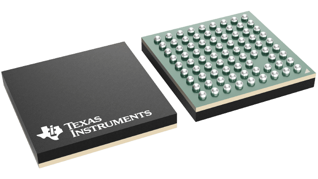
패키징 정보
| 패키지 | 핀 NFBGA (ZXH) | 80 |
| 작동 온도 범위(°C) -40 to 85 |
| 패키지 수량 | 캐리어 2,500 | LARGE T&R |
SN65LVDS302의 주요 특징
- Serial interface technology
- Compatible with FlatLink™3G such as SN65LVDS301
- Supports video interfaces up to 24-bit RGB data and 3 control bits received over 1, 2 or 3 SubLVDS differential lines
- SubLVDS differential voltage levels
- Up to 1.755-Gbps Data Throughput
- Three operating modes to conserve power
- Active mode QVGA: 17 mW
- Typical shutdown: 0.7 µW
- Typical standby mode: 27 µW Typical
- Bus-swap function for PCB-layout flexibility
- ESD rating > 4 kV (HBM)
- Pixel clock range of 4 MHz to 65 MHz
- Failsafe on all CMOS inputs
- Packaged in 5-mm × 5-mm nFBGA with 0.5-mm ball pitch
- Very low EMI meets SAE J1752/3 ’Kh’-spec
SN65LVDS302에 대한 설명
The SN65LVDS302 receiver de-serializes FlatLink™3G compliant serial input data to 27 parallel data outputs. The SN65LVDS302 receiver contains one shift register to load 30 bits from 1, 2 or 3 serial inputs and latches the 24 pixel bits and 3 control bits out to the parallel CMOS outputs after checking the parity bit. If the parity check confirms correct parity, the Channel Parity Error (CPE) output remains low. If a parity error is detected, the CPE output generates a high pulse while the data output bus disregards the newly-received pixel. Instead, the last data word is held on the output bus for another clock cycle.