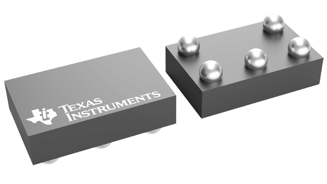
패키징 정보
| 패키지 | 핀 DSBGA (YZP) | 5 |
| 작동 온도 범위(°C) -40 to 85 |
| 패키지 수량 | 캐리어 3,000 | LARGE T&R |
SN74AUC1G08의 주요 특징
- Latch-Up Performance Exceeds 100 mA Per JESD 78, Class II
- ESD Protection Exceeds JESD 22
- 2000-V Human-Body Model (A114-A)
- 200-V Machine Model (A115-A)
- 1000-V Charged-Device Model (C101)
- Available in the Texas Instruments NanoFree™ Package
- Optimized for 1.8-V Operation and Is 3.6-V I/O Tolerant to Support Mixed-Mode Signal Operation
- Ioff Supports Partial-Power-Down Mode and Back Drive Protection
- Sub-1-V Operable
- Max tpd of 2.4 ns at 1.8 V
- Low Power Consumption, 10-µA Max ICC
- ±8-mA Output Drive at 1.8 V
SN74AUC1G08에 대한 설명
This single 2-input positive-AND gate is operational at 0.8-V to 2.7-V VCC, but is designed specifically for 1.65-V to 1.95-V VCC operation.
The SN74AUC1G08 device performs the Boolean function in positive logic.
NanoFree™ package technology is a major breakthrough in IC packaging concepts, using the die as the package.
This device is fully specified for partial-power-down applications using Ioff. The Ioff circuitry disables the outputs, preventing damaging current backflow through the device when it is powered down.