SBAS943A September 2018 – August 2019 ADS1284
PRODUCTION DATA.
- 1 Features
- 2 Applications
- 3 Description
- 4 Revision History
- 5 Pin Configuration and Functions
- 6 Specifications
- 7 Parameter Measurement Information
-
8 Detailed Description
- 8.1 Overview
- 8.2 Functional Block Diagram
- 8.3 Feature Description
- 8.4
Device Functional Modes
- 8.4.1 Synchronization (SYNC PIN and SYNC Command)
- 8.4.2 Reset (RESET Pin and Reset Command)
- 8.4.3 Master Clock Input (CLK)
- 8.4.4 Power-Down (PWDN Pin and STANDBY Command)
- 8.4.5 Power-On Sequence
- 8.4.6 DVDD Power Supply
- 8.4.7 Serial Interface
- 8.4.8 Data Format
- 8.4.9 Reading Data
- 8.4.10 One-Shot Operation
- 8.4.11 Offset and Full-Scale Calibration Registers
- 8.4.12 Calibration Commands (OFSCAL and GANCAL)
- 8.4.13 User Calibration
- 8.5
Programming
- 8.5.1
Commands
- 8.5.1.1 SDATAC Requirements
- 8.5.1.2 WAKEUP: Wake-Up From Standby Mode
- 8.5.1.3 STANDBY: Standby Mode
- 8.5.1.4 SYNC: Synchronize the Analog-to-Digital Conversion
- 8.5.1.5 RESET: Reset the Device
- 8.5.1.6 RDATAC: Read Data Continuous
- 8.5.1.7 SDATAC: Stop Read Data Continuous
- 8.5.1.8 RDATA: Read Data by Command
- 8.5.1.9 RREG: Read Register Data
- 8.5.1.10 WREG: Write to Register
- 8.5.1.11 OFSCAL: Offset Calibration
- 8.5.1.12 GANCAL: Gain Calibration
- 8.5.1
Commands
- 8.6
Register Maps
- 8.6.1
Register Descriptions
- 8.6.1.1 ID_CFG: ID_Configuration Register (address = 00h) [reset =x0h]
- 8.6.1.2 CONFIG0: Configuration Register 0 (address = 01h) [reset = 52h]
- 8.6.1.3 CONFIG1: Configuration Register 1 (address = 02h) [reset = 08h]
- 8.6.1.4 HPF0 and HPF1 Registers
- 8.6.1.5 OFC0, OFC1, OFC2 Registers
- 8.6.1.6 FSC0, FSC1, FSC2 Registers
- 8.6.1
Register Descriptions
- 9 Application and Implementation
- 10Device and Documentation Support
- 11Mechanical, Packaging, and Orderable Information
Package Options
Mechanical Data (Package|Pins)
- RHF|24
Thermal pad, mechanical data (Package|Pins)
Orderable Information
8.4.1.2 Continuous-Sync Mode
In continuous-sync mode, either a single synchronization pulse or a continuous synchronization clock may be applied. Use the SYNC pin in this mode. When a single sync pulse is applied (rising edge), the device resynchronizes the same way as pulse-sync mode. ADC re-synchronization occurs only when the time between SYNC rising edges is not an integer multiple of the conversion period. When resynchronization occurs, DRDY continues to toggle at the period of the date rate, and the DOUT output is held low until data are ready (63 DRDY periods later). At the 63rd reading, conversion data are valid, as shown in Figure 53.
If an additional pulse is applied to the SYNC pin, the elapsed time from the previous pulse must be an integral multiple of the output data rate otherwise re-synchronization results.
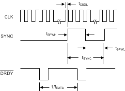
If a synchronization clock is applied to the SYNC pin, the device resynchronizes only under the condition tSYNC ≠ N / fDATA, where N = 1, 2, 3, and so on. When re-synchronized, DRDY continues to strobe, but the data on DOUT is held low until new data are valid after filter reset. If the period of the synchronizing clock matches an integral multiple of the data rate, the ADC does not re-synchronize. Note that the phase of the applied clock and output data rate (DRDY) is not aligned because of the initial delay of DRDY after the SYNC clock is first applied. Figure 54 shows the timing for continuous-sync mode.
 Figure 54. Continuous-Sync Timing With SYNC Clock
 Apply the synchronization clock after the continuous-sync mode is programmed. The first rising edge of SYNC then results in synchronization. Note that subsequent writes to any ADC register results in re-synchronization at the time of the register write operation. The re-synchronization leads to loss of the previous synchronization. Send the STANDBY command followed by the WAKEUP command to re-establish the previous synchronization. Re-synchronization occurs is valid as long as the time between the STANDBY and WAKEUP commands is not a multiple integer of the conversion period by at least one clock cycle.