SBAS943A September 2018 – August 2019 ADS1284
PRODUCTION DATA.
- 1 Features
- 2 Applications
- 3 Description
- 4 Revision History
- 5 Pin Configuration and Functions
- 6 Specifications
- 7 Parameter Measurement Information
-
8 Detailed Description
- 8.1 Overview
- 8.2 Functional Block Diagram
- 8.3 Feature Description
- 8.4
Device Functional Modes
- 8.4.1 Synchronization (SYNC PIN and SYNC Command)
- 8.4.2 Reset (RESET Pin and Reset Command)
- 8.4.3 Master Clock Input (CLK)
- 8.4.4 Power-Down (PWDN Pin and STANDBY Command)
- 8.4.5 Power-On Sequence
- 8.4.6 DVDD Power Supply
- 8.4.7 Serial Interface
- 8.4.8 Data Format
- 8.4.9 Reading Data
- 8.4.10 One-Shot Operation
- 8.4.11 Offset and Full-Scale Calibration Registers
- 8.4.12 Calibration Commands (OFSCAL and GANCAL)
- 8.4.13 User Calibration
- 8.5
Programming
- 8.5.1
Commands
- 8.5.1.1 SDATAC Requirements
- 8.5.1.2 WAKEUP: Wake-Up From Standby Mode
- 8.5.1.3 STANDBY: Standby Mode
- 8.5.1.4 SYNC: Synchronize the Analog-to-Digital Conversion
- 8.5.1.5 RESET: Reset the Device
- 8.5.1.6 RDATAC: Read Data Continuous
- 8.5.1.7 SDATAC: Stop Read Data Continuous
- 8.5.1.8 RDATA: Read Data by Command
- 8.5.1.9 RREG: Read Register Data
- 8.5.1.10 WREG: Write to Register
- 8.5.1.11 OFSCAL: Offset Calibration
- 8.5.1.12 GANCAL: Gain Calibration
- 8.5.1
Commands
- 8.6
Register Maps
- 8.6.1
Register Descriptions
- 8.6.1.1 ID_CFG: ID_Configuration Register (address = 00h) [reset =x0h]
- 8.6.1.2 CONFIG0: Configuration Register 0 (address = 01h) [reset = 52h]
- 8.6.1.3 CONFIG1: Configuration Register 1 (address = 02h) [reset = 08h]
- 8.6.1.4 HPF0 and HPF1 Registers
- 8.6.1.5 OFC0, OFC1, OFC2 Registers
- 8.6.1.6 FSC0, FSC1, FSC2 Registers
- 8.6.1
Register Descriptions
- 9 Application and Implementation
- 10Device and Documentation Support
- 11Mechanical, Packaging, and Orderable Information
Package Options
Mechanical Data (Package|Pins)
- RHF|24
Thermal pad, mechanical data (Package|Pins)
Orderable Information
8.3.3.2.1 Sinc Filter Section (sinx / x)
The sinc filter is a variable decimation rate, fifth-order, low-pass filter. Data are supplied to this section of the filter from the modulator at the rate of fMOD = fCLK / 4 (high-resolution mode) or fMOD = fCLK / 8 (low-power mode). The sinc filter attenuates high-frequency noise produced by the modulator and also reduces the data rate (decimation ratio) in proportion to the amount of filtering. The decimation ratio of the sinc filter effects the overall data rate of the converter. The sinc and sinc + FIR filter mode data rates are programmed by the DR[2:0] register bits. The sinc filter mode data rates are shown in Table 9.
Table 9. Sinc Filter Mode Data Rates
| DR[2:0] REGISTER | DECIMATION RATIO (N) | DATA RATE (SPS) | |
|---|---|---|---|
| HIGH-RESOLUTION MODE | LOW-POWER MODE | ||
| 000 | 128 | 64 | 8,000 |
| 001 | 64 | 32 | 16,000 |
| 010 | 32 | 16 | 32,000 |
| 011 | 16 | 8 | 64,000 |
| 100 | 8 | 4 | 128,000 |
Equation 9 shows the scaled Z-domain transfer function of the sinc filter.

where
- N = decimation ratio
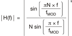
Equation 10 shows the frequency domain transfer function of the sinc filter.

where
- N = decimation ratio (see Table 9)
- fMOD = fCLK /4 (high-resolution mode) or fCLK / 8 (low-power mode)
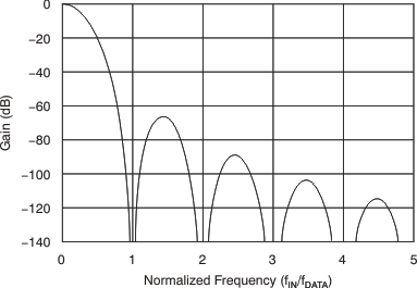
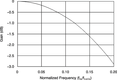
The sinc filter has notches (or zeros) that occur at the output data rate and multiples thereof. At these frequencies, the filter has zero gain. Figure 44 shows the frequency response of the sinc filter and Figure 45 shows the roll-off of the sinc filter.
 Figure 44. Sinc Filter Frequency Response
  Figure 45. Sinc Filter Roll-Off