SCAS931G May 2012 – January 2018 CDCM6208
PRODUCTION DATA.
- 1 Features
- 2 Applications
- 3 Description
- 4 Revision History
- 5 Pin Configuration and Functions
-
6 Specifications
- 6.1 Absolute Maximum Ratings
- 6.2 ESD Ratings
- 6.3 Recommended Operating Conditions
- 6.4 Thermal Information, Airflow = 0 LFM
- 6.5 Thermal Information, Airflow = 150 LFM
- 6.6 Thermal Information, Airflow = 250 LFM
- 6.7 Thermal Information, Airflow = 500 LFM
- 6.8 Single-Ended Input Characteristics (SI_MODE[1:0], SDI/SDA/PIN1, SCL/PIN4, SDO/ADD0/PIN2, SCS/ADD1/PIN3, STATUS1/PIN0, RESETN/PWR, PDN, SYNCN, REF_SEL)
- 6.9 Single-Ended Input Characteristics (PRI_REF, SEC_REF)
- 6.10 Differential Input Characteristics (PRI_REF, SEC_REF)
- 6.11 Crystal Input Characteristics (SEC_REF)
- 6.12 Single-Ended Output Characteristics (STATUS1, STATUS0, SDO, SDA)
- 6.13 PLL Characteristics
- 6.14 LVCMOS Output Characteristics
- 6.15 LVPECL (High-Swing CML) Output Characteristics
- 6.16 CML Output Characteristics
- 6.17 LVDS (Low-Power CML) Output Characteristics
- 6.18 HCSL Output Characteristics
- 6.19 Output Skew and Sync to Output Propagation Delay Characteristics
- 6.20 Device Individual Block Current Consumption
- 6.21 Worst Case Current Consumption
- 6.22 Timing Requirements, I2C Timing
- 6.23 Typical Characteristics
- 7 Parameter Measurement Information
-
8 Detailed Description
- 8.1 Overview
- 8.2 Functional Block Diagram
- 8.3
Feature Description
- 8.3.1 Typical Device Jitter
- 8.3.2 Universal Input Buffer (PRI_REF, SEC_REF)
- 8.3.3 VCO Calibration
- 8.3.4 Reference Divider (R)
- 8.3.5 Input Divider (M)
- 8.3.6 Feedback Divider (N)
- 8.3.7 Prescaler Dividers (PS_A, PS_B)
- 8.3.8 Phase Frequency Detector (PFD)
- 8.3.9 Charge Pump (CP)
- 8.3.10 Fractional Output Divider Jitter Performance
- 8.3.11 Device Block-Level Description
- 8.3.12 Device Configuration Control
- 8.3.13 Configuring the RESETN Pin
- 8.3.14 Preventing False Output Frequencies in SPI/I2C Mode at Start-Up
- 8.3.15 Input MUX and Smart Input MUX
- 8.4 Device Functional Modes
- 8.5 Programming
- 8.6 Register Maps
-
9 Application and Implementation
- 9.1 Application Information
- 9.2
Typical Applications
- 9.2.1 Design Requirements
- 9.2.2
Detailed Design Procedures
- 9.2.2.1 Jitter Considerations in SERDES Systems
- 9.2.2.2 Jitter Considerations in ADC and DAC Systems
- 9.2.2.3 Configuring the PLL
- 9.2.2.4 Programmable Loop Filter
- 9.2.2.5 Loop filter Component Selection
- 9.2.2.6 Device Output Signaling
- 9.2.2.7 Integer Output Divider (IO)
- 9.2.2.8 Fractional Output Divider (FOD)
- 9.2.2.9 Output Synchronization
- 9.2.2.10 Output Mux on Y4 and Y5
- 9.2.2.11 Staggered CLK Output Power Up for Power Sequencing of a DSP
- 10Power Supply Recommendations
- 11Layout
- 12Device and Documentation Support
- 13Mechanical, Packaging, and Orderable Information
Package Options
Mechanical Data (Package|Pins)
- RGZ|48
Thermal pad, mechanical data (Package|Pins)
- RGZ|48
Orderable Information
8.4.5.2.3 Block Write/Read Operation
The device supports a block write and block read operation. The host need only specify the lowest address of the sequence of addresses that the host needs to access. The CDCM6208 will automatically increment the internal register address pointer if the SCS pin remains low after the SPI port finishes the initial 32-bit transmission sequence. Each transmission of 16 bits (a data payload width) results in the device automatically incrementing the address pointer (provided the SCS pin remains active low for all sequences).
 Figure 42. CDCM6208 SPI Port Message Sequencing
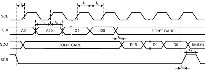
 Figure 43. CDCM6208 SPI Port Timing
Table 14. SPI Timing
| PARAMETER | MIN | TYP | MAX | UNIT | |
|---|---|---|---|---|---|
| fClock | Clock Frequency for the SCL | 20 | MHz | ||
| t1 | SPI_LE to SCL setup time | 10 | ns | ||
| t2 | SDI to SCL setup time | 10 | ns | ||
| t3 | SDO to SCL hold time | 10 | ns | ||
| t4 | SCL high duration | 25 | ns | ||
| t5 | SCL low duration | 25 | ns | ||
| t6 | SCL to SCS Setup time | 10 | ns | ||
| t7 | SCS Pulse Width | 20 | ns | ||
| t8 | SDI to SCL Data Valid (First Valid Bit after SCS) | 10 | ns | ||