SCAS931G May 2012 – January 2018 CDCM6208
PRODUCTION DATA.
- 1 Features
- 2 Applications
- 3 Description
- 4 Revision History
- 5 Pin Configuration and Functions
-
6 Specifications
- 6.1 Absolute Maximum Ratings
- 6.2 ESD Ratings
- 6.3 Recommended Operating Conditions
- 6.4 Thermal Information, Airflow = 0 LFM
- 6.5 Thermal Information, Airflow = 150 LFM
- 6.6 Thermal Information, Airflow = 250 LFM
- 6.7 Thermal Information, Airflow = 500 LFM
- 6.8 Single-Ended Input Characteristics (SI_MODE[1:0], SDI/SDA/PIN1, SCL/PIN4, SDO/ADD0/PIN2, SCS/ADD1/PIN3, STATUS1/PIN0, RESETN/PWR, PDN, SYNCN, REF_SEL)
- 6.9 Single-Ended Input Characteristics (PRI_REF, SEC_REF)
- 6.10 Differential Input Characteristics (PRI_REF, SEC_REF)
- 6.11 Crystal Input Characteristics (SEC_REF)
- 6.12 Single-Ended Output Characteristics (STATUS1, STATUS0, SDO, SDA)
- 6.13 PLL Characteristics
- 6.14 LVCMOS Output Characteristics
- 6.15 LVPECL (High-Swing CML) Output Characteristics
- 6.16 CML Output Characteristics
- 6.17 LVDS (Low-Power CML) Output Characteristics
- 6.18 HCSL Output Characteristics
- 6.19 Output Skew and Sync to Output Propagation Delay Characteristics
- 6.20 Device Individual Block Current Consumption
- 6.21 Worst Case Current Consumption
- 6.22 Timing Requirements, I2C Timing
- 6.23 Typical Characteristics
- 7 Parameter Measurement Information
-
8 Detailed Description
- 8.1 Overview
- 8.2 Functional Block Diagram
- 8.3
Feature Description
- 8.3.1 Typical Device Jitter
- 8.3.2 Universal Input Buffer (PRI_REF, SEC_REF)
- 8.3.3 VCO Calibration
- 8.3.4 Reference Divider (R)
- 8.3.5 Input Divider (M)
- 8.3.6 Feedback Divider (N)
- 8.3.7 Prescaler Dividers (PS_A, PS_B)
- 8.3.8 Phase Frequency Detector (PFD)
- 8.3.9 Charge Pump (CP)
- 8.3.10 Fractional Output Divider Jitter Performance
- 8.3.11 Device Block-Level Description
- 8.3.12 Device Configuration Control
- 8.3.13 Configuring the RESETN Pin
- 8.3.14 Preventing False Output Frequencies in SPI/I2C Mode at Start-Up
- 8.3.15 Input MUX and Smart Input MUX
- 8.4 Device Functional Modes
- 8.5 Programming
- 8.6 Register Maps
-
9 Application and Implementation
- 9.1 Application Information
- 9.2
Typical Applications
- 9.2.1 Design Requirements
- 9.2.2
Detailed Design Procedures
- 9.2.2.1 Jitter Considerations in SERDES Systems
- 9.2.2.2 Jitter Considerations in ADC and DAC Systems
- 9.2.2.3 Configuring the PLL
- 9.2.2.4 Programmable Loop Filter
- 9.2.2.5 Loop filter Component Selection
- 9.2.2.6 Device Output Signaling
- 9.2.2.7 Integer Output Divider (IO)
- 9.2.2.8 Fractional Output Divider (FOD)
- 9.2.2.9 Output Synchronization
- 9.2.2.10 Output Mux on Y4 and Y5
- 9.2.2.11 Staggered CLK Output Power Up for Power Sequencing of a DSP
- 10Power Supply Recommendations
- 11Layout
- 12Device and Documentation Support
- 13Mechanical, Packaging, and Orderable Information
Package Options
Mechanical Data (Package|Pins)
- RGZ|48
Thermal pad, mechanical data (Package|Pins)
- RGZ|48
Orderable Information
10.2 Device Power-Up Timing
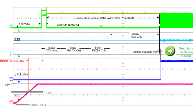
Before the device outputs turn on after power up, the device goes through the following initialization routine:
Table 43. Power-Up Timing Procedure
| STEP | DURATION | COMMENTS |
|---|---|---|
| Step 1: Power up ramp | Depends on customer supply ramp time | The POR monitor holds the device in power-down or reset until the VDD supply voltage reaches 1.06 V (min) to 1.26 V (max) |
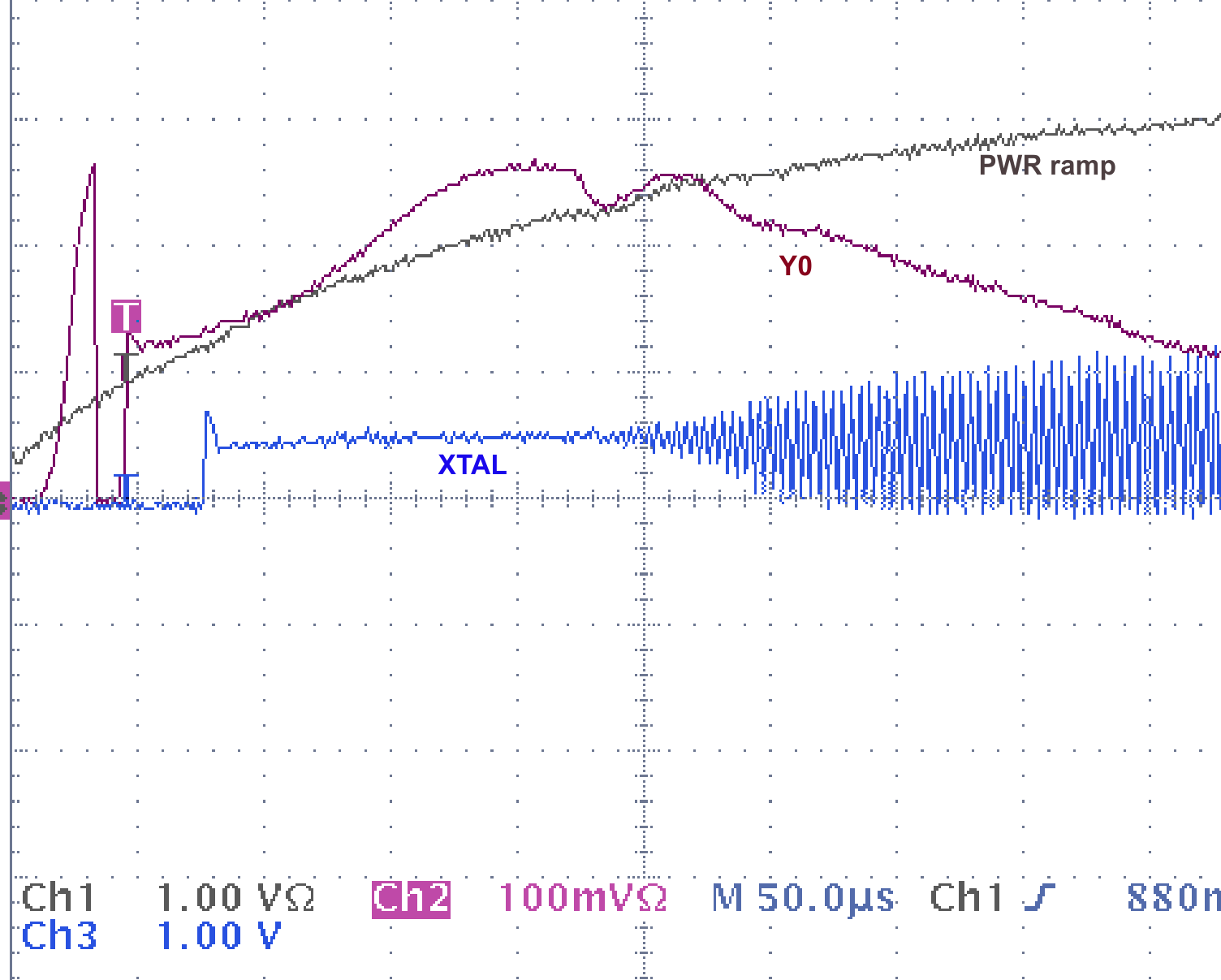
| Step 2: XO startup (if crystal is used) | Depends on XTAL. Could be several ms; For NX3225GA 25 MHz typical XTAL startup time measures 200 µs. |
This step assumes RESETN = 1 and PDN = 1.The XTAL startup time is the time it takes for the XTAL to oscillate with sufficient amplitude. The CDCM6208 has a built-in amplitude detection circuit, and holds the device in reset until the XTAL stage has sufficient swing. |
| Step 3: Ref Clock Counter | 64k Reference clock cycles at PFD input | This counter of 64 k clock cycles needs to expire before any further power-up step is done inside the device. This counter ensures that the input to the PFD from PRI or SEC input has stabilized in frequency. The duration of this step can range from 640 µs (fPFD= 100 MHz) to 8 sec (8 kHz PFD). |
| Step 4: FBCLK counter | 64k FBCLK cycles with CW=32; The duration is similar to Step 3, or can be more accurately estimated as: V1: approximately 64k x PS_A x N/2.48 GHz V2: approximately 64k x PS_A x N/3.05 GHz |
The Feedback counter delays the startup by another 64k PFD clock cycles. This is so that all counters are well initialized and also ensure additional timing margin for the reference clock to settle. This step can range from 640 µs (fPFD= 100 MHz) to 8 sec (fPFD= 8kHz). |
| Step 5: VCO calibration | 128k PFD reference clock cycles | This step calibrates the VCO to the exact frequency range, and takes exactly 128k PFD clock cycles. The duration can therefore range from 1280 µs (fPFD= 100 MHz) to 16 sec (f PFD= 8 KHz). |
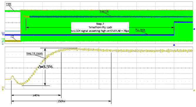
| Step 6: PLL lock time | approximately 3 x LBW | The Outputs turn on immediately after calibration. A small frequency error remains for the duration of approximately 3 x LBW (so in synthesizer mode typically 10 µs). The initial output frequency will be lower than the target output frequency, as the loop filter starts out initially discharged. |
| Step 7: PLL Lock indicator high | approximately 2305 PFD clock cycles | The PLL lock indicator if selected on output STATUS0 or STATUS1 will go high after approximately 2048 to 2560 PFD clock cycles to indicate PLL is now locked. |
 Figure 61. XTAL Start-Up Using NX3225GA 25 MHz (Step 2)
 Figure 62. PLL Lock Behavior (Step 6)