SCAS931G May 2012 – January 2018 CDCM6208
PRODUCTION DATA.
- 1 Features
- 2 Applications
- 3 Description
- 4 Revision History
- 5 Pin Configuration and Functions
-
6 Specifications
- 6.1 Absolute Maximum Ratings
- 6.2 ESD Ratings
- 6.3 Recommended Operating Conditions
- 6.4 Thermal Information, Airflow = 0 LFM
- 6.5 Thermal Information, Airflow = 150 LFM
- 6.6 Thermal Information, Airflow = 250 LFM
- 6.7 Thermal Information, Airflow = 500 LFM
- 6.8 Single-Ended Input Characteristics (SI_MODE[1:0], SDI/SDA/PIN1, SCL/PIN4, SDO/ADD0/PIN2, SCS/ADD1/PIN3, STATUS1/PIN0, RESETN/PWR, PDN, SYNCN, REF_SEL)
- 6.9 Single-Ended Input Characteristics (PRI_REF, SEC_REF)
- 6.10 Differential Input Characteristics (PRI_REF, SEC_REF)
- 6.11 Crystal Input Characteristics (SEC_REF)
- 6.12 Single-Ended Output Characteristics (STATUS1, STATUS0, SDO, SDA)
- 6.13 PLL Characteristics
- 6.14 LVCMOS Output Characteristics
- 6.15 LVPECL (High-Swing CML) Output Characteristics
- 6.16 CML Output Characteristics
- 6.17 LVDS (Low-Power CML) Output Characteristics
- 6.18 HCSL Output Characteristics
- 6.19 Output Skew and Sync to Output Propagation Delay Characteristics
- 6.20 Device Individual Block Current Consumption
- 6.21 Worst Case Current Consumption
- 6.22 Timing Requirements, I2C Timing
- 6.23 Typical Characteristics
- 7 Parameter Measurement Information
-
8 Detailed Description
- 8.1 Overview
- 8.2 Functional Block Diagram
- 8.3
Feature Description
- 8.3.1 Typical Device Jitter
- 8.3.2 Universal Input Buffer (PRI_REF, SEC_REF)
- 8.3.3 VCO Calibration
- 8.3.4 Reference Divider (R)
- 8.3.5 Input Divider (M)
- 8.3.6 Feedback Divider (N)
- 8.3.7 Prescaler Dividers (PS_A, PS_B)
- 8.3.8 Phase Frequency Detector (PFD)
- 8.3.9 Charge Pump (CP)
- 8.3.10 Fractional Output Divider Jitter Performance
- 8.3.11 Device Block-Level Description
- 8.3.12 Device Configuration Control
- 8.3.13 Configuring the RESETN Pin
- 8.3.14 Preventing False Output Frequencies in SPI/I2C Mode at Start-Up
- 8.3.15 Input MUX and Smart Input MUX
- 8.4 Device Functional Modes
- 8.5 Programming
- 8.6 Register Maps
-
9 Application and Implementation
- 9.1 Application Information
- 9.2
Typical Applications
- 9.2.1 Design Requirements
- 9.2.2
Detailed Design Procedures
- 9.2.2.1 Jitter Considerations in SERDES Systems
- 9.2.2.2 Jitter Considerations in ADC and DAC Systems
- 9.2.2.3 Configuring the PLL
- 9.2.2.4 Programmable Loop Filter
- 9.2.2.5 Loop filter Component Selection
- 9.2.2.6 Device Output Signaling
- 9.2.2.7 Integer Output Divider (IO)
- 9.2.2.8 Fractional Output Divider (FOD)
- 9.2.2.9 Output Synchronization
- 9.2.2.10 Output Mux on Y4 and Y5
- 9.2.2.11 Staggered CLK Output Power Up for Power Sequencing of a DSP
- 10Power Supply Recommendations
- 11Layout
- 12Device and Documentation Support
- 13Mechanical, Packaging, and Orderable Information
Package Options
Mechanical Data (Package|Pins)
- RGZ|48
Thermal pad, mechanical data (Package|Pins)
- RGZ|48
Orderable Information
8.3.15 Input MUX and Smart Input MUX
The Smart Input MUX supports auto-switching and manual-switching using control pin (and through register). The Smart Input MUX is designed such that glitches created during switching in both auto and manual modes are suppressed at the MUX output.
Table 5. Input MUX Selection
| SI_MODE1 PIN NO. 47 | REGISTER 4 BIT 13 SMUX_MODE_SEL | REGISTER 4 BIT 12 SMUX_REF_SEL | REF_SEL PIN NO. 6 | SELECTED INPUT | |
|---|---|---|---|---|---|
| 0 (SPI/I2C mode) | 0 | X | X | Auto Select Priority is given to Primary Reference input. | |
| 1 | 0 | 1 | Primary input | input select through SPI/I2C | |
| 1 | Secondary input | ||||
| 1 | 0 | Primary input | input select through external pin | ||
| 1 | Secondary input | ||||
| 1 (pin mode) | not available | 0 | Primary or Auto (see Table 6) | ||
| 1 | Secondary or Auto (see Table 6) | ||||
Example 1: An application desired to auto-select the clock reference in SPI/I2C mode. During production testing however, the system needs to force the device to use the primary followed by the secondary input. The settings would be as follows:
- Tie REF_SEL pin always high
- For primary clock input testing, use R4 [13:12] = 10
- For secondary clock input testing, set R4 [13:12] = 11.
- For the auto-mux setting in the final product shipment, set R3[13:12]=01 or 00
Example 2: The application wants to select the clock input manually without programming SPI/I2C. In this case, program R4[13:12] = 11, and select primary or secondary input by toggling REF_SEL low or high.
SmartMux input frequency limitation: In the automatic mode, the frequencies of both inputs to the smart mux (PRI_REF divided by R and SEC_REF) need to be similar; however, they can vary by up to 20%.
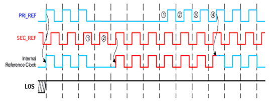
Switching behavior: The input clocks can have any phase. When switching happens between one input clock to the other, the phase of the output clock slowly transitions to the phase of the newly selected input clock. There will be no-phase jump at the output. The phase transition time to the new reference clock signal depends on the PLL loop filter bandwidth. Auto-switch assigns higher priority to PRI_REF and lower priority to SEC_REF. The timing diagram of an auto-switch at the input MUX is shown in Figure 37.
 Figure 37. Smart Input MUX Auto-Switch Mode Timing Diagram