SLAS837B April 2013 – January 2017 DAC3174
PRODUCTION DATA.
- 1 Features
- 2 Applications
- 3 Description
- 4 Revision History
- 5 Pin Configuration and Functions
-
6 Specifications
- 6.1 Absolute Maximum Ratings
- 6.2 ESD Ratings
- 6.3 Recommended Operating Conditions
- 6.4 Thermal Information
- 6.5 Electrical Characteristics: DC Specifications
- 6.6 Electrical Characteristics: AC Specifications
- 6.7 Electrical Characteristics: Digital Specifications
- 6.8 Timing Requirements
- 6.9 Typical Characteristics
-
7 Detailed Description
- 7.1 Overview
- 7.2 Functional Block Diagrams
- 7.3 Feature Description
- 7.4 Device Functional Modes
- 7.5 Programming
- 7.6
Register Maps
- 7.6.1 config0 Register (address = 0x00) [reset = 0x44FC]
- 7.6.2 config 1 Register (address = 0x01) [reset = 0x600E]
- 7.6.3 config2 Register (address = 0x02) [reset = 0x3FFF]
- 7.6.4 config3 Register (address = 0x03) [reset = 0x0000]
- 7.6.5 config4 Register (address = 0x04) [reset = 0x0000]
- 7.6.6 config5 Register (address = 0x05) [reset = 0x0000]
- 7.6.7 config6 Register (address = 0x06) [reset = 0x0000]
- 7.6.8 config7 Register (address = 0x07) [reset = 0xFFFF]
- 7.6.9 config8 Register (address = 0x08) [reset = 0x4000]
- 7.6.10 config9 Register (address = 0x09) [reset = 0x8000]
- 7.6.11 config10 Register (address = 0x0A) [reset = 0xF080]
- 7.6.12 config11 Register (address = 0x0B) [reset = 0x1111]
- 7.6.13 config12 Register (address = 0x0C) [reset = 0x3A7A]
- 7.6.14 config13 Register (address = 0x0D) [reset = 0x36B6]
- 7.6.15 config14 Register (address = 0x0E) [reset = 0x2AEA]
- 7.6.16 config15 Register (address = 0x0F) [reset = 0x0545]
- 7.6.17 config16 Register (address = 0x10) [reset = 0x0585]
- 7.6.18 config17 Register (address = 0x11) [reset = 0x0949]
- 7.6.19 config18 Register (address = 0x12) [reset = 0x1515]
- 7.6.20 config19 Register (address = 0x13) [reset = 0x3ABA]
- 7.6.21 config20 Register (address = 0x14) [reset = 0x0000]
- 7.6.22 config21 Register (address = 0x15) [reset = 0xFFFF]
- 7.6.23 config22 Register (address = 0x16) [reset = N/A]
- 7.6.24 config23 Register (address = 0x17) [reset = N/A]
- 7.6.25 config24 Register (address = 0x18) [reset = N/A]
- 7.6.26 config25 Register (address = 0x19) [reset = N/A]
- 7.6.27 config127 Register (address = 0x7F) [reset = 0x0045]
- 8 Application and Implementation
- 9 Power Supply Recommendations
- 10Layout
- 11Device and Documentation Support
- 12Mechanical, Packaging, and Orderable Information
Package Options
Mechanical Data (Package|Pins)
- RGC|64
Thermal pad, mechanical data (Package|Pins)
- RGC|64
Orderable Information
6 Specifications
6.1 Absolute Maximum Ratings
over operating free-air temperature range (unless otherwise noted)(1)| MIN | MAX | UNIT | ||
|---|---|---|---|---|
| Supply voltage | VDDA33 to GND | –0.5 | 4 | V |
| VDDA18 to GND | –0.5 | 2.3 | ||
| CLKVDD18 to GND | –0.5 | 2.3 | ||
| IOVDD to GND | –0.5 | 4 | ||
| DIGVDD18 to GND | –0.5 | 2.3 | ||
| Terminal voltage | CLKVDD18 to DIGVDD18 | –0.5 | 0.5 | V |
| VDDA18 to DIGVDD18 | –0.5 | 0.5 | ||
| DA[6:0]P, DA[6:0]N, DB[6:0]P, DB[6:0]N, D[13:0]P, D[13:0]N, DATACLKP, DATACLKN, DA_CLKP, DA_CLKPN, DB_CLKP, DB_CLKN, SYNCP, SYNCN to GND | –0.5 | DIGVDD18 + 0.5 | ||
| DACCLKP, DACCLKN, ALIGNP, ALIGNN | –0.5 | CLKVDD18 + 0.5 | ||
| TXENABLE, ALARM, SDO, SDIO, SCLK, SDENB, RESETB to GND | –0.5 | IOVDD + 0.5 | ||
| IOUTAP, IOUTAN, IOUTBP, IOUTBN to GND | –0.7 | 1.4 | ||
| EXTIO, BIASJ to GND | –0.5 | VDDA33 + 0.5 | ||
| Temperature | Operating ambient free-air, TA | –40 | 85 | °C |
| Maximum junction, TJ | 125 | |||
| Storage, Tstg | –65 | 150 | ||
(1) Stresses beyond those listed under Absolute Maximum Ratings may cause permanent damage to the device. These are stress ratings only, which do not imply functional operation of the device at these or any other conditions beyond those indicated under Recommended Operating Conditions. Exposure to absolute-maximum-rated conditions for extended periods may affect device reliability.
6.2 ESD Ratings
| VALUE | UNIT | |||
|---|---|---|---|---|
| V(ESD) | Electrostatic discharge | Human-body model (HBM), per ANSI/ESDA/JEDEC JS-001(1) | ±2000 | V |
| Charged-device model (CDM), per JEDEC specification JESD22-C101(2) | ±500 | |||
(1) JEDEC document JEP155 states that 500-V HBM allows safe manufacturing with a standard ESD control process.
(2) JEDEC document JEP157 states that 250-V CDM allows safe manufacturing with a standard ESD control process.
6.3 Recommended Operating Conditions
| MIN | NOM | MAX | UNIT | ||
|---|---|---|---|---|---|
| CLKVDD18 | Clock buffer supply | 1.71 | 1.8 | 1.89 | V |
| DIGVDD18 | Digital supply | 1.71 | 1.8 | 1.89 | V |
| VDDA18 | 1.8-V analog supply | 1.71 | 1.8 | 1.89 | V |
| VFUSE | Fuse bank supply | 1.71 | 1.8 | 1.89 | V |
| IOVDD | IO supply(1) | 1.71 | 3.45 | V | |
| VDDA33 | 3.3-V analog supply | 3.15 | 3.3 | 3.45 | V |
| TA | Operating ambient free-air temperature | –40 | 25 | 85 | °C |
| TJ | Operating junction temperature(2) | 105 | °C | ||
(1) Sets CMOS IO voltage levels; nominal 1.8 V, 2.5 V, or 3.3 V.
(2) Prolonged use at this junction temperature may increase the device failure-in-time (FIT) rate.
6.4 Thermal Information
| THERMAL METRIC(1) | DAC3174 | UNIT | |
|---|---|---|---|
| RGC (VQFN) | |||
| 64 PINS | |||
| RθJA | Junction-to-ambient thermal resistance | 23 | °C/W |
| RθJC(top) | Junction-to-case (top) thermal resistance | 7.6 | °C/W |
| RθJB | Junction-to-board thermal resistance | 2.8 | °C/W |
| ψJT | Junction-to-top characterization parameter | 0.1 | °C/W |
| ψJB | Junction-to-board characterization parameter | 2.8 | °C/W |
| RθJC(bot) | Junction-to-case (bottom) thermal resistance | 0.2 | °C/W |
(1) For more information about traditional and new thermal metrics, see the Semiconductor and IC Package Thermal Metrics application report.
6.5 Electrical Characteristics: DC Specifications
Typical values at TA = 25°C, full temperature range is TMIN = –40°C to TMAX = 85°C, DAC sample rate = 500 MSPS, 50% clock duty cycle, VDDA33 = IOVDD = 3.3 V, VDDA18 = CLKVDD18 = DIGVDD18 = 1.8 V, and IOUTFS = 20 mA (unless otherwise noted).| PARAMETER | TEST CONDITIONS | MIN | TYP | MAX | UNIT | |
|---|---|---|---|---|---|---|
| Resolution | 14 | Bits | ||||
| DC ACCURACY | ||||||
| DNL | Differential nonlinearity | 1 LSB = IOUTFS / 214 | ±1 | LSB | ||
| INL | Integral nonlinearity | 1 LSB = IOUTFS / 214 | ±2 | LSB | ||
| ANALOG OUTPUTS | ||||||
| Coarse gain linearity | ±0.4 | LSB | ||||
| Offset error | Midcode offset | 0.01 | %FSR | |||
| Gain error | With external reference | ±2 | %FSR | |||
| With internal reference | ±2 | |||||
| Gain mismatch | With internal reference | –2 | 2 | %FSR | ||
| Minimum full-scale output current | Nominal full-scale current, IOUTFS = 16 × IBAIS current |
2 | mA | |||
| Maximum full-scale output current | Nominal full-scale current, IOUTFS = 16 × IBAIS current |
20 | mA | |||
| Output compliance | IOUTFS = 20 mA | –0.5 | 1 | V | ||
| Output resistance | 300 | kΩ | ||||
| Output capacitance | 5 | pF | ||||
| REFERENCE OUTPUT | ||||||
| VREF | Reference output voltage | 1.14 | 1.2 | 1.26 | V | |
| Reference output current | 100 | nA | ||||
| REFERENCE INPUT | ||||||
| VEXTIO input voltage | External reference mode | 0.1 | 1.2 | 1.25 | V | |
| Input resistance | 1 | MΩ | ||||
| Small-signal bandwidth | 500 | kHz | ||||
| Input capacitance | 100 | pF | ||||
| TEMPERATURE COEFFICIENTS | ||||||
| Offset drift | ±1 | ppm of FSR/°C | ||||
| Gain drift | With external reference | ±15 | ||||
| With internal reference | ±30 | |||||
| Reference voltage drift | ±8 | ppm /°C | ||||
| POWER CONSUMPTION | ||||||
| IVDDA33 | 3.3-V analog supply current | MODE 1, fDAC = 491.52 MSPS, QMC on, IF = 20 MHz | 52 | 59 | mA | |
| MODE 2, fDAC = 320 MSPS, QMC on, IF = 20 MHz |
51 | |||||
| MODE 3, sleep mode, fDAC = 491.52 MSPS, DAC in sleep mode | 2.6 | |||||
| MODE 4, power-down mode, no clock, DAC in sleep mode | 1.6 | 4 | ||||
| ICLKVDD18 | 1.8-V clock and analog supply current (CLKVDD18 and VDDA18) | MODE 1, fDAC = 491.52 MSPS, QMC on, IF = 20 MHz | 49 | 57 | mA | |
| MODE 2, fDAC = 320 MSPS, QMC on, IF = 20 MHz |
38 | |||||
| MODE 3, sleep mode, fDAC = 491.52 MSPS, DAC in sleep mode | 43 | |||||
| MODE 4, power-down mode, no clock, DAC in sleep mode | 1.8 | 4 | ||||
| IDIGVDD18 | 1.8-V digital supply current (DIGVDD18 and VFUSE) |
MODE 1, fDAC = 491.52 MSPS, QMC on, IF = 20 MHz | 115 | 130 | mA | |
| MODE 2, fDAC = 320 MSPS, QMC on, IF = 20 MHz |
87 | |||||
| MODE 3, sleep mode, fDAC = 491.52 MSPS, DAC in sleep mode | 110 | |||||
| MODE 4, power-down mode, no clock, DAC in sleep mode | 0.7 | 3 | ||||
| IIOVDD | 1.8-V IO supply current | MODE 1, fDAC = 491.52 MSPS, QMC on, IF = 20 MHz | 0.002 | 0.015 | mA | |
| MODE 2, fDAC = 320 MSPS, QMC on, IF = 20 MHz |
0.002 | |||||
| MODE 3, sleep mode, fDAC = 491.52 MSPS, DAC in sleep mode | 0.003 | |||||
| MODE 4, power-down mode, no clock, DAC in sleep mode | 0.003 | 0.015 | ||||
| Pdis | Total power dissipation | MODE 1, fDAC = 491.52 MSPS, QMC on, IF = 20 MHz | 464 | 530 | mW | |
| MODE 2, fDAC = 320 MSPS, QMC on, IF = 20 MHz |
396 | |||||
| MODE 3, sleep mode, fDAC = 491.52 MSPS, DAC in sleep mode | 284 | |||||
| MODE 4, power-down mode, no clock, DAC in sleep mode | 10 | 26 | ||||
| PSRR | Power-supply rejection ratio | DC tested | –0.4 | 0.4 | %FSR/V | |
6.6 Electrical Characteristics: AC Specifications
Typical values at T A = 25°C, full temperature range is TMIN = –40°C to TMAX = 85°C, DAC sample rate = 500 MSPS, 50% clock duty cycle, VDDA33 = IOVDD = 3.3 V, VDDA18 = CLKVDD18 = DIGVDD18 = 1.8 V, and IOUT FS = 20 mA (unless otherwise noted).| PARAMETER | TEST CONDITIONS | MIN | TYP | MAX | UNIT | |
|---|---|---|---|---|---|---|
| ANALOG OUTPUT | ||||||
| fDAC | Maximum sample rate | 500 | MSPS | |||
| ts(DAC) | Output settling time to 0.1% | Transition: Code 0x0000 to 0x3FFF | 11 | ns | ||
| tPD | Output propagation delay | Does not include digital latency | 2 | ns | ||
| tr(IOUT) | Output rise time | 10% to 90% | 200 | ps | ||
| tf(IOUT) | Output fall time | 90% to 10% | 200 | ps | ||
| Digital latency | Length of delay from DAC pin inputs to DATA at output pins. In normal operation mode including the latency of FIFO. | 26 | DACCLK | |||
| AC PERFORMANCE | ||||||
| SFDR | Spurious free dynamic | fDAC = 500 MSPS, fout = 10.1 MHz | 82 | dBc | ||
| fDAC = 500 MSPS, fout = 20.1 MHz | 78 | |||||
| fDAC = 500 MSPS, fout = 70.1 MHz | 74 | |||||
| IMD3 | Intermodulation distortion | fDAC = 500 MSPS, fout = 10.1 ±0.5 MHz | 84 | dBc | ||
| fDAC = 500 MSPS, fout = 20.1 ±0.5 MHz | 84 | |||||
| fDAC = 500 MSPS, fout = 70.1 ±0.5 MHz | 75 | |||||
| fDAC = 500 MSPS, fout = 150.1 ±0.5 MHz | 63 | |||||
| NSD | Noise spectral density | fDAC = 500 MSPS, fout = 10.1 MHz | 160 | dBc/Hz | ||
| fDAC = 500 MSPS, fout = 20.1 MHz | 157 | |||||
| fDAC = 500 MSPS, fout = 70.1 MHz | 155 | |||||
| ACLR | Adjacent channel leakage ratio | fDAC = 491.52 MSPS, fout = 30.72 MHz, WCDMA TM1 | 78 | dBc | ||
| f AC = 491.52 MSPS, fout = 153.6 MHz, WCDMA TM1 | 74 | |||||
6.7 Electrical Characteristics: Digital Specifications
Typical values at T A = 25°C, full temperature range is T MIN = –40°C to T MAX = 85°C, DAC sample rate = 500 MSPS, 50% clock duty cycle, VDDA33 = IOVDD = 3.3 V, VDDA18 = CLKVDD18 = DIGVDD18 = 1.8 V, and IOUT FS = 20 mA (unless otherwise noted).| PARAMETERS | TEST CONDITIONS | MIN | TYP | MAX | UNIT | |||
|---|---|---|---|---|---|---|---|---|
| CMOS DIGITAL INPUTS (RESETB, SDENB, SCLK, SDIO, TXENABLE) | ||||||||
| VIH | High-level input voltage | IOVDD = 3.3 V, 2.5 V, or 1.8 V | IOVDD × 0.6 | V | ||||
| VIL | Low-level input voltage | IOVDD = 3.3 V, 2.5 V, or 1.8 V | 0.25 × IOVDD | V | ||||
| IIH | High-level input current | IOVDD = 3.3 V, 2.5 V, or 1.8 V | –40 | 40 | µA | |||
| IIL | Low-level input current | IOVDD = 3.3 V, 2.5 V, or 1.8 V | –40 | 40 | µA | |||
| DIGITAL OUTPUTS – CMOS INTERFACE (SDOUT, SDIO) | ||||||||
| VOH | High-level output voltage | IOVDD = 3.3 V, 2.5 V, or 1.8 V | 0.85 × IOVDD | V | ||||
| VOL | Low-level output voltage | 0.125 × IOVDD | V | |||||
| LVPECL INPUTS – (DACCLKx, ALIGNx) | ||||||||
| VCM | LVPECL input common-mode voltage | 0.5 | V | |||||
| VIDIFF | Differential input peak-to-peak voltage | 0.4 | 1 | V | ||||
| LVDS INTERFACE (DATA[13:0]x, DA[6:0]x , DB[6:0]x , DA_CLKx, DB_CLKx, DATACLKx, SYNCx) | ||||||||
| VA,B+ | Logic high differential input voltage threshold | 175 | mV | |||||
| VA,B– | Logic low differential input voltage threshold | –175 | mV | |||||
| VCOM | LVDS input common-mode voltage | 1 | 1.2 | 2 | V | |||
| ZT | Internal termination | 85 | 110 | 135 | Ω | |||
| CL | LVDS input capacitance | 2 | pF | |||||
6.8 Timing Requirements
Typical values at T A = 25°C, full temperature range is T MIN = –40°C to T MAX = 85°C, DAC sample rate = 500 MSPS, 50% clock duty cycle, VDDA33 = IOVDD = 3.3 V, VDDA18 = CLKVDD18 = DIGVDD18 = 1.8 V, and IOUT FS = 20 mA (unless otherwise noted).| MIN | TYP | MAX | UNIT | |||||
|---|---|---|---|---|---|---|---|---|
| SERIAL PORT TIMING | ||||||||
| ts(SENDB) | Setup time, SDENB to rising edge of SCLK | 20 | ns | |||||
| ts(SDIO) | Setup time, SDIO to rising edge of SCLK | 10 | ns | |||||
| th(SDIO) | Hold time, SDIO from rising edge of SCLK | 5 | ns | |||||
| t(SCLK) | Period of SCLK | 100 | ns | |||||
| t(SCLKH) | High time of SCLK | 40 | ns | |||||
| t(SCLKL) | Low time of SCLK | 40 | ns | |||||
| td(DATA) | Data output delay after falling edge of SCLK | 10 | ns | |||||
| TRESET | Minimum RESTB pulse duration | 25 | ns | |||||
| LVDS INPUT TIMING | ||||||||
| ts(DATA) | Setup time | D[x..0] valid to DATACLK rising or falling edge for single bus single clock mode ; DA/DB[x…0] valid to DB_CLK rising or falling edge for dual bus single clock mode; DA[x..0] valid to DA_CLK rising or falling edge, and DB[x…0] valid for DB_CLK rising or falling edge for dual bus dual clock mode |
config3 Setting | ps | ||||
| datadly | clkdly | |||||||
| 0 | 0 | –20 | ||||||
| 0 | 1 | –120 | ||||||
| 0 | 2 | –220 | ||||||
| 0 | 3 | –310 | ||||||
| 0 | 4 | –390 | ||||||
| 0 | 5 | –480 | ||||||
| 0 | 6 | –560 | ||||||
| 0 | 7 | –630 | ||||||
| 1 | 0 | 70 | ||||||
| 2 | 0 | 150 | ||||||
| 3 | 0 | 230 | ||||||
| 4 | 0 | 330 | ||||||
| 5 | 0 | 430 | ||||||
| 6 | 0 | 530 | ||||||
| 7 | 0 | 620 | ||||||
| th(DATA) | Hold time | D[x..0] valid to DATACLK rising or falling edge for single bus single clock mode; DA/DB[x…0] valid to DB_CLK rising or falling edge for dual bus single clock mode; DA[x..0] valid to DA_CLK rising or falling edge, and DB[x…0] valid for DB_CLK rising or falling edge for dual bus dual clock mode. |
config3 Setting | ps | ||||
| datadly | clkdly | |||||||
| 0 | 0 | 310 | ||||||
| 0 | 1 | 390 | ||||||
| 0 | 2 | 480 | ||||||
| 0 | 3 | 560 | ||||||
| 0 | 4 | 650 | ||||||
| 0 | 5 | 740 | ||||||
| 0 | 6 | 850 | ||||||
| 0 | 7 | 930 | ||||||
| 1 | 0 | 200 | ||||||
| 2 | 0 | 100 | ||||||
| 3 | 0 | 20 | ||||||
| 4 | 0 | –60 | ||||||
| 5 | 0 | –140 | ||||||
| 6 | 0 | –220 | ||||||
| 7 | 0 | –290 | ||||||
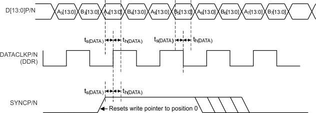 Figure 1. Input Data Timing for Single-Bus, Single-Clock Mode
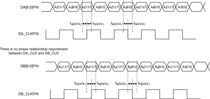 Figure 2. Input Data Timing for Dual-Bus, Dual-Clock Mode
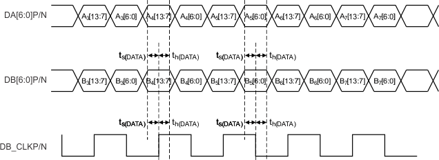 Figure 3. Input Data Timing for Dual-Bus, Single-Clock Mode
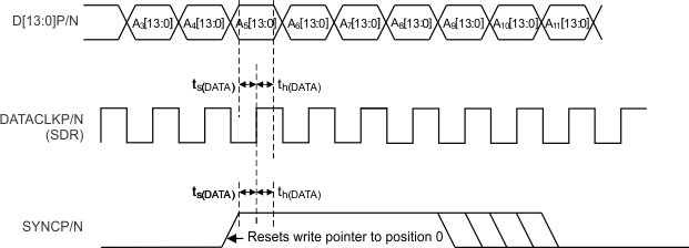 Figure 4. Input Data Timing for Single-Channel, Single Data Rate (SDR) Mode
6.9 Typical Characteristics
All plots are at 25°C, nominal supply voltages, fDAC = 500 MSPS, 50% clock duty cycle, 0-dBFS input signal, and 20-mA full-scale output current (unless otherwise noted).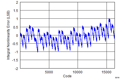 Figure 5. Integral Nonlinearity
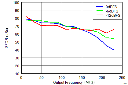 Figure 7. SFDR vs Output Frequency Over Input Scale
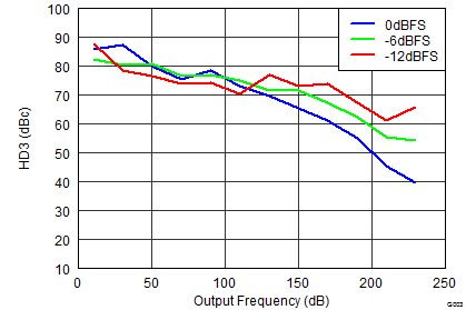 Figure 9. Third-Order Harmonic Distortion
vs Output Frequency Over Input Scale
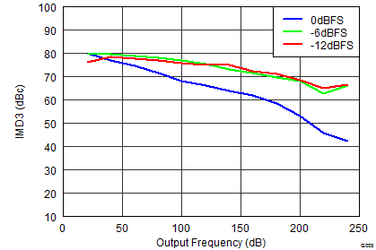 Figure 11. IMD3 vs Output Frequency Over Input Scale
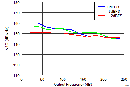 Figure 13. NSD vs Output Frequency Over Input Scale
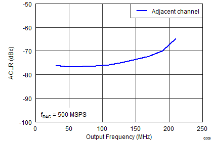 Figure 15. ACLR (Adjacent Channel) vs Output Frequency
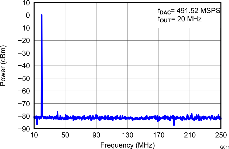
| IF = 20 MHz |
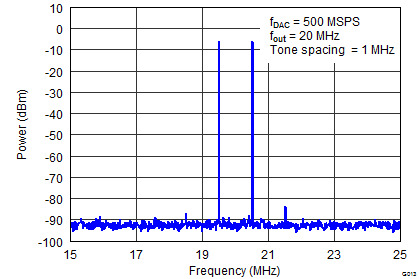
| IF = 20 MHz |
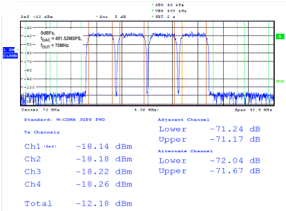 Figure 21. Four-Carrier WCDMA Test Mode 1
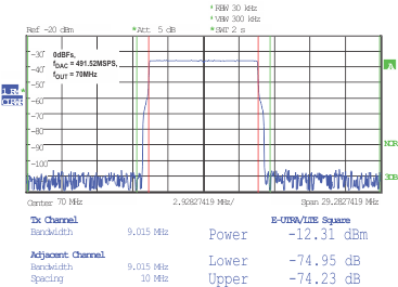 Figure 23. ACPR – LTE 10-MHz FDD E-TM 1.1
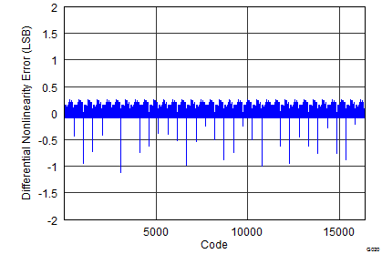 Figure 6. Differential Nonlinearity
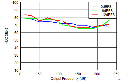 Figure 8. Second-Order Harmonic Distortion
vs Output Frequency Over Input Scale
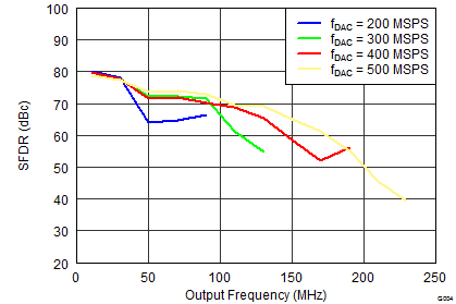 Figure 10. SFDR vs Output Frequency Over fDAC
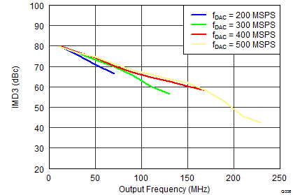 Figure 12. IMD3 vs Output Frequency Over fDAC
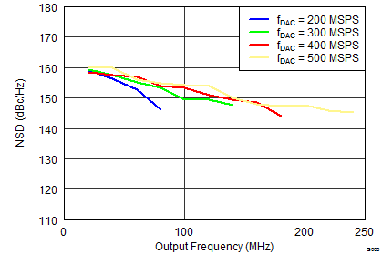 Figure 14. NSD vs Output Frequency Over fDAC
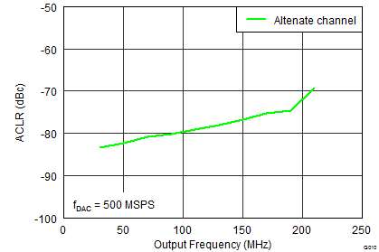 Figure 16. ACLR (Alternate Channel) vs Output Frequency
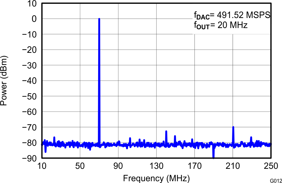
| IF = 70 MHz |
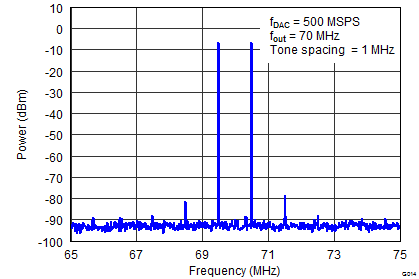
| IF = 70 MHz |
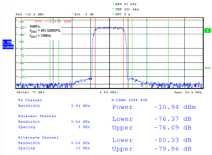 Figure 22. Single-Carrier WCDMA Test Mode 1
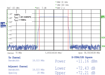 Figure 24. ACPR – LTE 20-MHz FDD E-TM 1.1