DLPS095A November 2017 – February 2023 DLP650LE
PRODUCTION DATA
- 1 Features
- 2 Applications
- 3 Description
- 4 Revision History
- 5 Pin Configuration and Functions
-
6 Specifications
- 6.1 Absolute Maximum Ratings
- 6.2 Storage Conditions
- 6.3 ESD Ratings
- 6.4 Recommended Operating Conditions
- 6.5 Thermal Information
- 6.6 Electrical Characteristics
- 6.7 Capacitance at Recommended Operating Conditions
- 6.8 Timing Requirements
- 6.9 Window Characteristics
- 6.10 System Mounting Interface Loads
- 6.11 Micromirror Array Physical Characteristics
- 6.12 Micromirror Array Optical Characteristics
- 6.13 Chipset Component Usage Specification
- 7 Detailed Description
- 8 Application and Implementation
- 9 Power Supply Recommendations
- 10Device and Documentation Support
- 11Mechanical, Packaging, and Orderable Information
Package Options
Mechanical Data (Package|Pins)
- FYL|149
Thermal pad, mechanical data (Package|Pins)
Orderable Information
6.12 Micromirror Array Optical Characteristics
Table 6-4 Micromirror Array Optical Characteristics
| PARAMETER | MIN | NOM | MAX | UNIT | ||
|---|---|---|---|---|---|---|
| Mirror Tilt angle, variation device to device#DLPS08581 #T4989946-28#T4989946-29#DLPS0728306 | 11 | 12 | 13 | degrees | ||
| Number of out-of-specification micromirrors#T4589833-6 | Adjacent micromirrors | 0 | micromirrors | |||
| Non-adjacent micromirrors | 10 | |||||
(1) Measured relative to the plane formed by the overall micromirror array
(2) Variation can occur between any two individual micromirrors located on the same device or located on different devices.
(3) Additional variation exists between the micromirror array and the package datums. See the package drawing.
(4) See #DLPS0728274.
(5) An out-of-specification micromirror is defined as a micromirror that is unable to transition between the two landed states.
Note: This number is specified under conditions described above and deviations from the specified conditions could result in decreased efficiency.
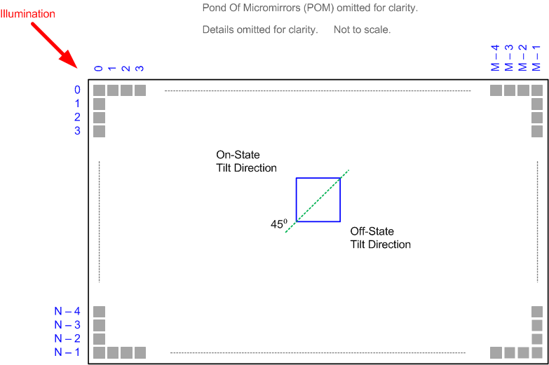
 Figure 6-9 Micromirror Landed Orientation and Tilt
Refer to GUID-F2939A35-FB9B-45B9-ADD1-AC11F215A958.html#GUID-F2939A35-FB9B-45B9-ADD1-AC11F215A958 table for M, N, and P specifications.