SNLS656D August 2020 – December 2023 DP83TD510E
PRODUCTION DATA
- 1
- 1 Features
- 2 Applications
- 3 Description
- 4 Pin Configuration and Functions
- 5 Specifications
-
6 Detailed Description
- 6.1 Overview
- 6.2 Functional Block Diagram
- 6.3
Feature Description
- 6.3.1 Auto-Negotiation (Speed Selection)
- 6.3.2 Repeater Mode
- 6.3.3 Media Converter
- 6.3.4 Clock Output
- 6.3.5 Media Independent Interface (MII)
- 6.3.6 Reduced Media Independent Interface (RMII)
- 6.3.7 RMII Low Power 5-MHz Mode
- 6.3.8 RGMII Interface
- 6.3.9 Serial Management Interface
- 6.3.10 Extended Register Space Access
- 6.3.11 Loopback Modes
- 6.3.12 BIST Configurations
- 6.3.13 Cable Diagnostics
- 6.4 Device Functional Modes
- 6.5 Programming
- 6.6 MMD Register Address Map
- 6.7 DP83TD510E Registers
- 7 Application and Implementation
- 8 Device and Documentation Support
- 9 Revision History
- 10Mechanical, Packaging, and Orderable Information
Package Options
Mechanical Data (Package|Pins)
- RHB|32
Thermal pad, mechanical data (Package|Pins)
- RHB|32
Orderable Information
3 Description
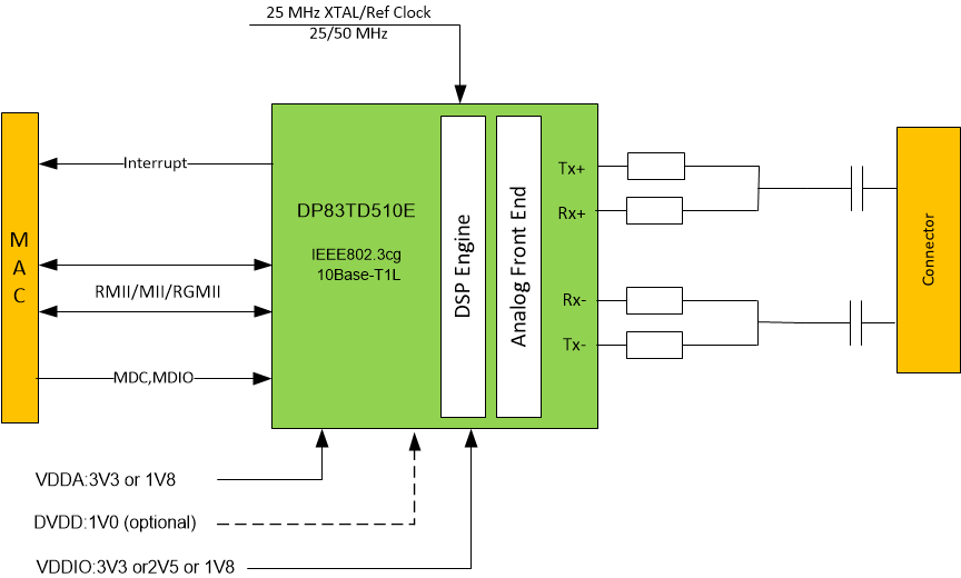
The DP83TD510E is an ultra-low power Ethernet physical layer transceiver compliant with the IEEE 802.3cg 10Base-T1L specification. The PHY has very low noise coupled receiver architecture enabling long cable reach and very low power dissipation. The DP83TD510E has external MDI termination to support intrinsic safety requirements. It interfaces with MAC layer through MII, Reduced MII (RMII) , RGMII, and RMII low power 5-MHz master mode. It also supports RMII back-to-back mode for applications that require cable reach extension beyond 2000 meters. It supports a 25MHz reference clock output to clock other modules on the system. The DP83TD510E offers integrated cable diagnostic tools; built-in self-test, and loopback capabilities for ease of design or debug.
| PART NUMBER | PACKAGE (1) | BODY SIZE (NOM) |
|---|---|---|
| DP83TD510E | QFN (32) | 5.00 mm × 5.00 mm |
 DP83TD510E Application Diagram