SNLS656D August 2020 – December 2023 DP83TD510E
PRODUCTION DATA
- 1
- 1 Features
- 2 Applications
- 3 Description
- 4 Pin Configuration and Functions
- 5 Specifications
-
6 Detailed Description
- 6.1 Overview
- 6.2 Functional Block Diagram
- 6.3
Feature Description
- 6.3.1 Auto-Negotiation (Speed Selection)
- 6.3.2 Repeater Mode
- 6.3.3 Media Converter
- 6.3.4 Clock Output
- 6.3.5 Media Independent Interface (MII)
- 6.3.6 Reduced Media Independent Interface (RMII)
- 6.3.7 RMII Low Power 5-MHz Mode
- 6.3.8 RGMII Interface
- 6.3.9 Serial Management Interface
- 6.3.10 Extended Register Space Access
- 6.3.11 Loopback Modes
- 6.3.12 BIST Configurations
- 6.3.13 Cable Diagnostics
- 6.4 Device Functional Modes
- 6.5 Programming
- 6.6 MMD Register Address Map
- 6.7 DP83TD510E Registers
- 7 Application and Implementation
- 8 Device and Documentation Support
- 9 Revision History
- 10Mechanical, Packaging, and Orderable Information
Package Options
Mechanical Data (Package|Pins)
- RHB|32
Thermal pad, mechanical data (Package|Pins)
- RHB|32
Orderable Information
6.4.1 Straps Configuration
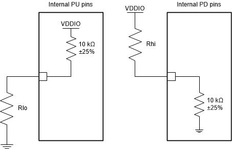
The DP83TD510E uses many of the functional pins as strap options to place the device into specific modes of operation. The values of these pins are sampled at power up or hard reset. During software resets, the strap options are internally reloaded from the values sampled at power up or hard reset. The strap option pin assignments are defined below. Configuration of the device may be done through the strap pins or through the management register interface. A pullup resistor or a pulldown resistor of suggested values may be used to set the voltage ratio of the strap pin input and the supply to select one of the possible selected modes. The MAC interface pins must support I/O voltages of 3.3 V, 2.5 V, and 1.8 V. As the strap inputs are implemented on these pins, the straps must also support operation at 3.3-V, 2.5-V, and 1.8-V supplies depending on what voltage was selected for I/O. All strap pins have two levels.
PHY offers interal PU or PD resistor for the default strap configuration and eliminates need for external resistor. External resistor for strap is needed only when default configuratoin needs to be be changed.
 Figure 6-10 Strap Circuit
| MODE | IDEAL RESISTORS | |
|---|---|---|
| Rhi (kΩ) | Rlo (kΩ) | |
| 0 | OPEN | 2.49 |
| 1 | 2.49 | OPEN |