SNLS656D August 2020 – December 2023 DP83TD510E
PRODUCTION DATA
- 1
- 1 Features
- 2 Applications
- 3 Description
- 4 Pin Configuration and Functions
- 5 Specifications
-
6 Detailed Description
- 6.1 Overview
- 6.2 Functional Block Diagram
- 6.3
Feature Description
- 6.3.1 Auto-Negotiation (Speed Selection)
- 6.3.2 Repeater Mode
- 6.3.3 Media Converter
- 6.3.4 Clock Output
- 6.3.5 Media Independent Interface (MII)
- 6.3.6 Reduced Media Independent Interface (RMII)
- 6.3.7 RMII Low Power 5-MHz Mode
- 6.3.8 RGMII Interface
- 6.3.9 Serial Management Interface
- 6.3.10 Extended Register Space Access
- 6.3.11 Loopback Modes
- 6.3.12 BIST Configurations
- 6.3.13 Cable Diagnostics
- 6.4 Device Functional Modes
- 6.5 Programming
- 6.6 MMD Register Address Map
- 6.7 DP83TD510E Registers
- 7 Application and Implementation
- 8 Device and Documentation Support
- 9 Revision History
- 10Mechanical, Packaging, and Orderable Information
Package Options
Mechanical Data (Package|Pins)
- RHB|32
Thermal pad, mechanical data (Package|Pins)
- RHB|32
Orderable Information
6.3.8 RGMII Interface
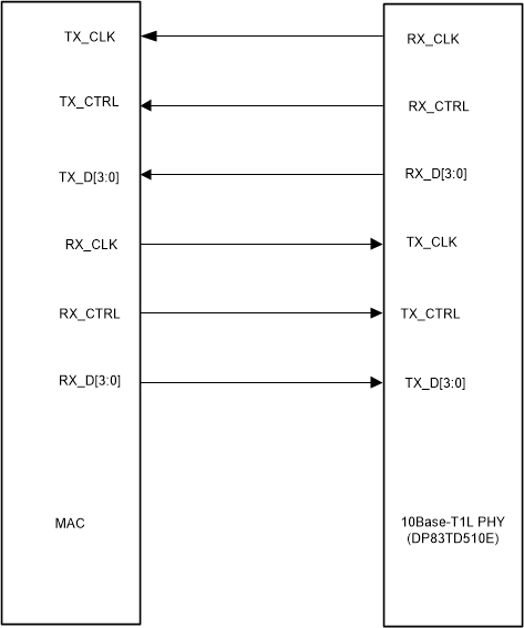
DP83TD510E offers RGMII MAC interface as defined by Reduced Gigabit Media Independent Interface (RGMII) as specified by RGMII version 2.0. RGMII is designed to reduce the number of pins required to connect the MAC and PHY. To accomplish this goal, the control signals are multiplexed. Both rising and falling edges of the clock are used to sample the control signal pin on the transmit and receive paths. For 10-Mbps operation, RX_CLK and TX_CLK operate at 2.5 MHz. The timing specifications are relaxed compared to RGMII 1000M interface specifations. Refer to timing sections on timing specifications for this mode.
Function | PINs |
Data Signals | TX_D[3:0] |
RX_D[3:0] | |
Transmit and Recieve Clocks | TX_CLK |
RX_CLK | |
Transmit and Recieve Signals | TX_CTRL |
RX_CTRL |
 Figure 6-7 RGMII Signalling.