SLVSDS7B August 2019 – November 2019 DRV8876
PRODUCTION DATA.
- 1 Features
- 2 Applications
- 3 Description
- 4 Revision History
- 5 Pin Configuration and Functions
- 6 Specifications
- 7 Detailed Description
- 8 Application and Implementation
- 9 Power Supply Recommendations
- 10Layout
- 11Device and Documentation Support
- 12Mechanical, Packaging, and Orderable Information
Package Options
Refer to the PDF data sheet for device specific package drawings
Mechanical Data (Package|Pins)
- RGT|16
- PWP|16
Thermal pad, mechanical data (Package|Pins)
Orderable Information
8.2.1.2.3.1 Steady-State Thermal Performance
"Steady-state" conditions assume that the motor driver operates with a constant RMS current over a long period of time.Figure 21, Figure 22, Figure 23, and Figure 24 show how RθJA and ΨJB (junction-to-board characterization parameter) change depending on copper area, copper thickness, and number of layers of the PCB for the HTSSOP package. More copper area, more layers, and thicker copper planes decrease RθJA and ΨJB, which indicate better thermal performance from the PCB layout.
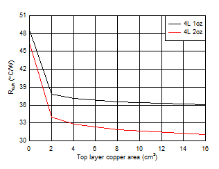 Figure 21. HTSSOP, 4-layer PCB junction-to-ambient thermal resistance vs copper area
 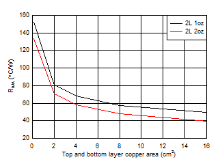 Figure 23. HTSSOP, 2-layer PCB junction-to-ambient thermal resistance vs copper area
 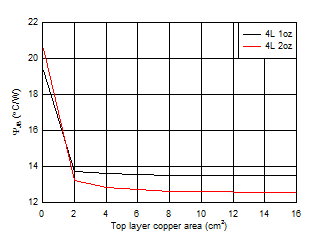 Figure 22. HTSSOP, 4-layer PCB junction-to-board characterization parameter vs copper area
 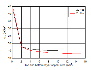 Figure 24. HTSSOP, 2-layer PCB junction-to-board characterization parameter vs copper area
 Figure 25 and Figure 26 show how RθJA and ΨJB vary with the bottom layer copper area for the VQFN package mounted on a 2-layer board. In the case of the 4-layer board, the top-layer copper area cannot be varied. Figure 29 and Figure 30 at 1000 s show the steady-state RθJA of the 4-layer board.
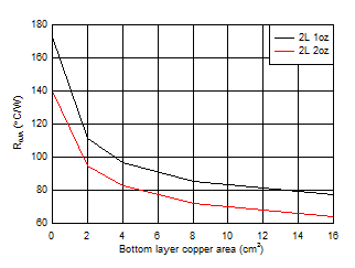 Figure 25. VQFN, 2-layer PCB junction-to-ambient thermal resistance vs copper area
 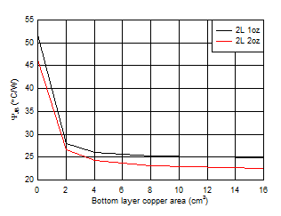 Figure 26. VQFN, 2-layer PCB junction-to-board characterization parameter vs copper area