SNLS426F August 2012 – November 2018 DS125BR800
PRODUCTION DATA.
- 1 Features
- 2 Applications
- 3 Description
- 4 Revision History
- 5 Description (cont.)
- 6 Pin Configuration and Functions
- 7 Specifications
- 8 Detailed Description
- 9 Application and Implementation
- 10Power Supply Recommendations
- 11Layout
- 12Device and Documentation Support
- 13Mechanical, Packaging, and Orderable Information
Package Options
Mechanical Data (Package|Pins)
- NJY|54
Thermal pad, mechanical data (Package|Pins)
Orderable Information
10.1 3.3-V or 2.5-V Supply Mode Operation
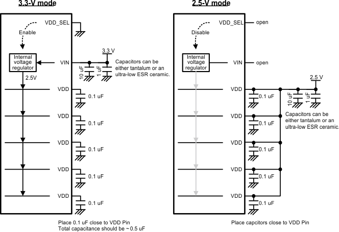
The DS125BR800 has an optional internal voltage regulator to provide the 2.5-V supply to the device. In 3.3-V mode operation, the VIN pin = 3.3 V is used to supply power to the device. The internal regulator will provide the 2.5 V to the VDD pins of the device and a 0.1-µF cap is needed at each of the 5 VDD pins for power supply de-coupling (total capacitance should be ≤0.5 µF), and the VDD pins should be left open. The VDD_SEL pin must be tied to GND to enable the internal regulator. In 2.5-V mode operation, the VIN pin should be left open and 2.5-V supply must be applied to the 5 VDD pins to power the device. The VDD_SEL pin must be left open (no connect) to disable the internal regulator.
The DS125BR800 has an optional internal voltage regulator to provide the 2.5 V supply to the device. In 3.3-V Mode operation, the VIN pin = 3.3 V is used to supply power to the device. The internal regulator will provide the 2.5 V to the VDD pins of the device and a 0.1-µF cap is needed at each of the 5 VDD pins for power supply decoupling (total capacitance should be ≤0.5 µF), and the VDD pins should be left open. The VDD_SEL pin must be tied to GND to enable the internal regulator. In 2.5-V Mode operation, the VIN pin should be left open and 2.5-V supply must be applied to the 5 VDD pins to power the device. The VDD_SEL pin must be left open (no connect) to disable the internal regulator.
 Figure 26. 3.3-V or 2.5-V Supply Connection Diagram