SNLS426F August 2012 – November 2018 DS125BR800
PRODUCTION DATA.
- 1 Features
- 2 Applications
- 3 Description
- 4 Revision History
- 5 Description (cont.)
- 6 Pin Configuration and Functions
- 7 Specifications
- 8 Detailed Description
- 9 Application and Implementation
- 10Power Supply Recommendations
- 11Layout
- 12Device and Documentation Support
- 13Mechanical, Packaging, and Orderable Information
Package Options
Mechanical Data (Package|Pins)
- NJY|54
Thermal pad, mechanical data (Package|Pins)
Orderable Information
7.7 Timing Requirements
| MIN | TYP | MAX | UNIT | |||
|---|---|---|---|---|---|---|
| SERIAL BUS INTERFACE TIMING SPECIFICATIONS | ||||||
| FSMB | Bus Operating Frequency(1) | ENSMB = VDD (Slave Mode) | 400 | kHz | ||
| ENSMB = FLOAT (Master Mode) | 280 | 400 | 520 | kHz | ||
| TBUF | Bus Free Time Between Stop and Start Condition | 1.3 | µs | |||
| THD:STA | Hold time after (Repeated) Start Condition. After this period, the first clock is generated. | At IPULLUP, Max | 0.6 | µs | ||
| TSU:STA | Repeated Start Condition Setup Time | 0.6 | µs | |||
| TSU:STO | Stop Condition Setup Time | 0.6 | µs | |||
| THD:DAT | Data Hold Time | 0 | ns | |||
| TSU:DAT | Data Setup Time | 100 | ns | |||
| TLOW | Clock Low Period | 1.3 | µs | |||
| THIGH | Clock High Period | (2) | 0.6 | 50 | µs | |
| tF | Clock/Data Fall Time | (2) | 300 | ns | ||
| tR | Clock/Data Rise Time | (2) | 300 | ns | ||
| tPOR | Time in which a device must be operational after power-on reset | (2)(3) | 500 | ms | ||
(1) In Master Mode, a serial EEPROM with a minimum rating of 520 KHz is required.
(2) Compliant to SMBus 2.0 physical layer specification. See System Management Bus (SMBus) Specification Version 2.0, section 3.1.1 SMBus common AC specifications for details.
(3) Specified by Design. Parameter not tested in production.
 Figure 1. CML Output and Rise and FALL Transition Time
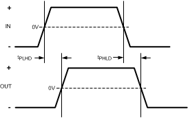
  Figure 2. Propagation Delay Timing Diagram
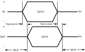
  Figure 3. Transmit IDLE-DATA and DATA-IDLE Response Time
  Figure 4. SMBus Timing Parameters