SNLS346C August 2011 – June 2014 DS90UR903Q-Q1 , DS90UR904Q-Q1
PRODUCTION DATA.
- 1 Features
- 2 Applications
- 3 Description
- 4 Revision History
- 5 Pin Configuration and Functions
-
6 Specifications
- 6.1 Absolute Maximum Ratings
- 6.2 Handling Ratings
- 6.3 Recommended Operating Conditions
- 6.4 Thermal Information
- 6.5 Electrical Characteristics
- 6.6 Recommended Serializer Timing for PCLK
- 6.7 Serial Control Bus AC Timing Specifications (SCL, SDA) - I2C Compliant (See )
- 6.8 Serial Control Bus DC Characteristics (SCL, SDA) - I2C Compliant
- 6.9 Serializer Switching Characteristics
- 6.10 Deserializer Switching Characteristics
- 6.11 Typical Characteristics
- 7 Detailed Description
- 8 Application and Implementation
- 9 Power Supply Recommendations
- 10Layout
- 11Device and Documentation Support
- 12Mechanical, Packaging, and Orderable Information
Package Options
Mechanical Data (Package|Pins)
- RHS|48
Thermal pad, mechanical data (Package|Pins)
- RHS|48
Orderable Information
8 Application and Implementation
8.1 Application Information
The DS90UR903Q/904Q chipset is intended for interface between a host (graphics processor) and a Display. It supports a 21 bit parallel video bus for 18-bit color depth (RGB666) display format. In a RGB666 configuration, 18 color bits (R[5:0], G[5:0], B[5:0]), Pixel Clock (PCLK) and three control bits (VS, HS and DE) are supported across the serial link.
The DS90UR903Q Serializer accepts a 21-bit parallel data bus. The parallel data is converted into a single differential link. The DS90UR904Q Deserializer extracts the clock/control information from the incoming data stream and reconstructs the 21-bit parallel data.
Camera applications are also supported by the DS90UR903Q/904Q chipset. The host controller/processsor is connected to the deserializer, while the CMOS image sensor provides data to the serializer.
8.2 Typical Applications
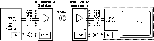 Figure 26. Typical Display System Diagram
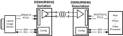 Figure 27. Typical Camera System Diagram
8.2.1 Design Requirements
For the typical design applications, use the following as input parameters.
Table 5. Design Parameters
| Design Parameter | Example Value |
|---|---|
| VDDIO | 1.8 V or 3.3 V |
| VDDn | 1.8 V |
| AC Coupling Capacitor for DOUT± and RIN± | 100 nF |
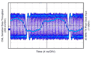
| PCLK Frequency | 43 MHz |
8.2.2 Detailed Design Procedure
8.2.2.1 Typical Application Connection
Figure 28 shows a typical connection of the DS90UR903Q Serializer for an 18-bit application. The CML outputs require 0.1 μF AC coupling capacitors to the line. The line driver includes internal termination. Bypass capacitors are placed near the power supply Terminals. System GPO (General Purpose Output) signals control the PDB and MODE Terminals. The interface to the host is with 1.8 V LVCMOS levels, thus the VDDIO Terminal is connected also to the 1.8V rail. The optional Serial Bus control is used in this example, thus SCL and SDA are connected to the system and the ID[x] Terminal is connected to a resistor divider.
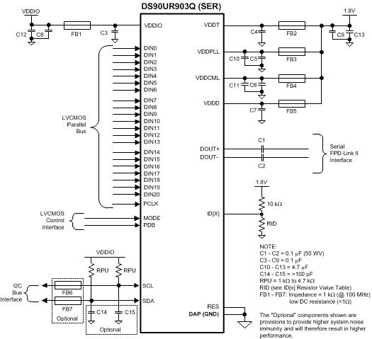 Figure 28. DS90UR903Q Typical Connection Diagram — Pin Control
40-Pin WQFN (RTA Package)
Figure 29 shows a typical connection of the DS90UR904Q Deserializer for an 18-bit application. The CML inputs utilize 0.1 μF coupling capacitors to the line and the receiver provides internal termination. Bypass capacitors are placed near the power supply Terminals. System GPO (General Purpose Output) signals control the PDB and the MODE Terminals. The interface to the target display is with 3.3V LVCMOS levels, thus the VDDIO Terminal is connected to the 3.3 V rail. The optional Serial Bus control is used in this example, thus SCL and SDA are connected to the system and the ID[x] Terminal is connected to a resistor divider. LOCK is monitored by a system GPI (General Purpose Input).
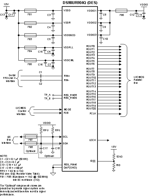 Figure 29. DS90UR904Q Typical Connection Diagram — Pin Control
48-Pin WQFN (RHS Package)
8.2.2.2 AC Coupling
The SER/DES supports only AC-coupled interconnects through an integrated DC balanced decoding scheme. External AC coupling capacitors must be placed in series in the FPD-Link II signal path as illustrated in Figure 30.
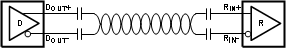 Figure 30. AC-Coupled Connection
For high-speed FPD-Link II transmissions, the smallest available package should be used for the AC coupling capacitor. This will help minimize degradation of signal quality due to package parasitics. The I/O’s require a 100 nF AC coupling capacitors to the line.
8.2.2.3 Power Up Requirements and PDB PIN
When power is applied, the VDDIO supply needs to reach the expected operating voltage (1.8V or 3.3V) before the other supplies (VDDn) begin to ramp. It is also required to delay and release the PDB input signal after VDD (VDDn and VDDIO) power supplies have settled to the recommended operating voltages. A external RC network can be connected to the PDB pin to ensure PDB arrives after all the VDD have stabilized.
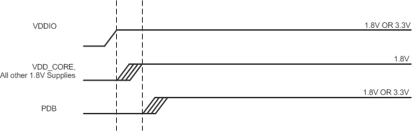 Figure 31. Power Up Sequence
8.2.2.4 Transmission Media
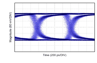
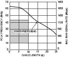
The Ser/Des chipset is intended to be used over a wide variety of balanced cables depending on distance and signal quality requirements. The Ser/Des employ internal termination providing a clean signaling environment. The interconnect for FPD-Link II interface should present a differential impedance of 100 Ohms. Use of cables and connectors that have matched differential impedance will minimize impedance discontinuities. Shielded or un-shielded cables may be used depending upon the noise environment and application requirements. The chipset's optimum cable drive performance is achieved at 43 MHz at 10 meters length. The maximum signaling rate increases as the cable length decreases. Therefore, the chipset supports 50 MHz at shorter distances. Other cable parameters that may limit the cable's performance boundaries are: cable attenuation, near-end crosstalk and pair-to-pair skew.
For obtaining optimal performance, we recommend:
- Use Shielded Twisted Pair (STP) cable
- 100Ω differential impedance and 24 AWG (or lower AWG) cable
- Low skew, impedance matched
- Ground and/or terminate unused conductors
Figure 32 shows the Typical Performance Characteristics demonstrating various lengths and data rates using Rosenberger HSD and Leoni DACAR 538 Cable.
8.2.2.5 Serial Interconnect Guidelines
For full details, see the Channel-Link PCB and Interconnect Design-In Guidelines (literature number SNLA008) and the Transmission Line RAPIDESIGNER Operation and Applications Guide (literature number SNLA035).
- Use 100Ω coupled differential pairs
- Use the S/2S/3S rule in spacings
- S = space between the pair
- 2S = space between pairs
- 3S = space to LVCMOS signal
- Minimize the number of Vias
- Use differential connectors when operating above 500Mbps line speed
- Maintain balance of the traces
- Minimize skew within the pair
Additional general guidance can be found in the LVDS Owner’s Manual (literature number SNLA187), which is available in PDF format from the TI LVDS & CML Solutions web site.