SNLS346C August 2011 – June 2014 DS90UR903Q-Q1 , DS90UR904Q-Q1
PRODUCTION DATA.
- 1 Features
- 2 Applications
- 3 Description
- 4 Revision History
- 5 Pin Configuration and Functions
-
6 Specifications
- 6.1 Absolute Maximum Ratings
- 6.2 Handling Ratings
- 6.3 Recommended Operating Conditions
- 6.4 Thermal Information
- 6.5 Electrical Characteristics
- 6.6 Recommended Serializer Timing for PCLK
- 6.7 Serial Control Bus AC Timing Specifications (SCL, SDA) - I2C Compliant (See )
- 6.8 Serial Control Bus DC Characteristics (SCL, SDA) - I2C Compliant
- 6.9 Serializer Switching Characteristics
- 6.10 Deserializer Switching Characteristics
- 6.11 Typical Characteristics
- 7 Detailed Description
- 8 Application and Implementation
- 9 Power Supply Recommendations
- 10Layout
- 11Device and Documentation Support
- 12Mechanical, Packaging, and Orderable Information
Package Options
Mechanical Data (Package|Pins)
- RHS|48
Thermal pad, mechanical data (Package|Pins)
- RHS|48
Orderable Information
7 Detailed Description
7.1 Overview
The DS90UR903Q/904Q FPD-Link II chipset is intended for video display applications. The Serializer/ Deserializer chipset operates from a 10 MHz to 43 MHz pixel clock frequency. The DS90UR903Q transforms a 21-bit wide parallel LVCMOS data bus into a single high-speed differential pair. The high-speed serial bit stream contains an embedded clock and DC-balance information which enhances signal quality to support AC coupling. The DS90UR904Q receives the single serial data stream and converts it back into a 21-bit wide parallel data bus.
7.2 Functional Block Diagram
7.2.1 Typical Application Diagram
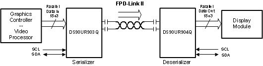 Figure 20. Typical Application Circuit
7.2.2 Block Diagrams
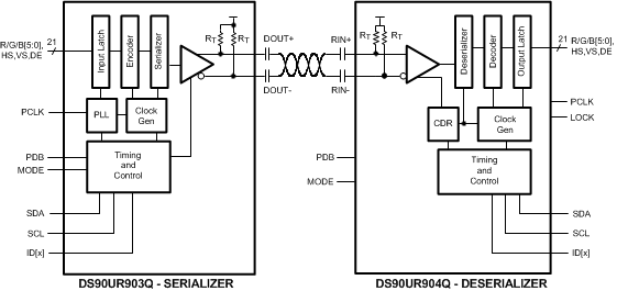 Figure 21. Block Diagram
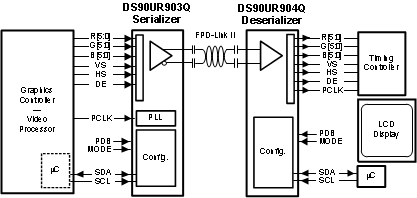 Figure 22. Application Block Diagram
7.3 Feature Description
7.3.1 Serial Frame Format
The DS90UR903Q/904Q chipset will transmit and receive a pixel of data in the following format:
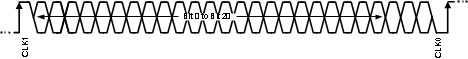 Figure 23. Serial Bitstream for 28-bit Symbol
The High Speed Serial Channel is a 28-bit symbol composed of 21 bits of data containing video data & control information transmitted from Serializer to Deserializer. CLK1 and CLK0 represent the embedded clock in the serial stream. CLK1 is always HIGH and CLK0 is always LOW. This data payload is optimized for signal transmission over an AC coupled link. Data is randomized, balanced and scrambled.
7.3.2 Signal Quality Enhancers
7.3.2.1 Des - Receiver Input Equalization (EQ)
The receiver inputs provided input equalization filter in order to compensate for loss from the media. The level of equalization is controlled via register setting.
7.3.3 Emi Reduction
7.3.3.1 Des - Receiver Staggered Output
The Receiver staggered outputs allows for outputs to switch in a random distribution of transitions within a defined window. Outputs transitions are distributed randomly. This minimizes the number of outputs switching simultaneously and helps to reduce supply noise. In addition it spreads the noise spectrum out reducing overall EMI.
7.3.3.2 Des Spread Spectrum Clocking
The DS90UR904Q parallel data and clock outputs have programmable SSCG ranges from 9 kHz–66 kHz and ±0.5%–±2% from 20 MHz to 43 MHz. The modulation rate and modulation frequency variation of output spread is controlled through the SSC control registers.
7.4 Device Functional Modes
7.4.1 LVCMOS VDDIO Option
1.8V or 3.3V SER Inputs and DES Outputs are user selectable to provide compatibility with 1.8V and 3.3V system interfaces.
7.4.2 Powerdown
The SER has a PDB input pin to ENABLE or Powerdown the device. The modes can be controlled by the host and is used to disable the Link to save power when the remote device is not operational. An auto mode is also available. In this mode, the PDB pin is tied High and the SER switches over to an internal oscillator when the PCLK stops or not present. When a PCLK starts again, the SER will then lock to the valid input PCLK and transmits the data to the DES. In powerdown mode, the high-speed driver outputs are static (High).
The DES has a PDB input pin to ENABLE or Powerdown the device. This pin can be controlled by the system and is used to disable the DES to save power. An auto mode is also available. In this mode, the PDB pin is tied High and the DES will enter powerdown when the serial stream stops. When the serial stream starts up again, the DES will lock to the input stream and assert the LOCK pin and output valid data. In powerdown mode, the Data and PCLK outputs are set by the OSS_SEL control register.
7.4.3 Pixel Clock Edge Select (TRFB/RRFB)
The TRFB/RRFB selects which edge of the Pixel Clock is used. For the SER, this register determines the edge that the data is latched on. If TRFB register is 1, data is latched on the Rising edge of the PCLK. If TRFB register is 0, data is latched on the Falling edge of the PCLK. For the DES, this register determines the edge that the data is strobed on. If RRFB register is 1, data is strobed on the Rising edge of the PCLK. If RRFB register is 0, data is strobed on the Falling edge of the PCLK.
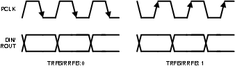 Figure 24. Programmable PCLK Strobe Select
7.5 Programming
7.5.1 Description of Serial Control Bus
An integrated I2C slave controller is embedded in each of the DS90UR903Q Serializer and DS90UR904Q Deserializer. It must be used to access and program the extra features embedded within the configuration registers. Refer to Table 3 and Table 4 for details of control registers.
7.5.2 ID[X] Address Decoder
The ID[x] pin is used to decode and set the physical slave address of the Serializer/Deserializer (I2C only) to allow up to six devices on the bus using only a single pin. The pin sets one of six possible addresses for each Serializer/Deserializer device. The pin must be pulled to VDD (1.8V, NOT VDDIO)) with a 10 kΩ resistor and a pull down resistor (RID) of the recommended value to set the physical device address. The recommended maximum resistor tolerance is 0.1% worst case (0.2% total tolerance).
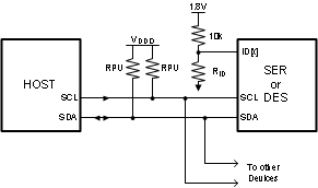 Figure 25. Serial Control Bus Connection
Table 1. ID[x] Resistor Value – DS90UR903Q
| ID[x] RESISTOR VALUE - DS90UR903Q Ser | ||
|---|---|---|
| RESISTOR RID Ω (±0.1%) | ADDRESS 7'b(11) | ADDRESS 8'b 0 APPENDED (WRITE) |
| 0 GND |
7b' 101 1000 (h'58) | 8b' 1011 0000 (h'B0) |
| 2.0k | 7b' 101 1001 (h'59) | 8b' 1011 0010 (h'B2) |
| 4.7k | 7b' 101 1010 (h'5A) | 8b' 1011 0100 (h'B4) |
| 8.2k | 7b' 101 1011 (h'5B) | 8b' 1011 0110 (h'B6) |
| 12.1k | 7b' 101 1100 (h'5C) | 8b' 1011 1000 (h'B8) |
| 39.0k | 7b' 101 1110 (h'5E) | 8b' 1011 1100 (h'BC) |
Table 2. ID[x] Resistor Value – DS90UR904Q
| ID[x] RESISTOR VALUE - DS90UR904Q Des | ||
|---|---|---|
| RESISTOR RID Ω (±0.1%) | ADDRESS 7'b(11) | ADDRESS 8'b 0 APPENDED (WRITE) |
| 0 GND |
7b' 110 0000 (h'60) | 8b' 1100 0000 (h'C0) |
| 2.0k | 7b' 110 0001 (h'61) | 8b' 1100 0010 (h'C2) |
| 4.7k | 7b' 110 0010 (h'62) | 8b' 1100 0100 (h'C4) |
| 8.2k | 7b' 110 0011 (h'63) | 8b' 1101 0110 (h'C6) |
| 12.1k | 7b' 110 0100 (h'64) | 8b' 1101 1000 (h'C8) |
| 39.0k | 7b' 110 0110 (h'66) | 8b' 1100 1100 (h'CC) |
7.6 Register Maps
Table 3. DS90UR903Q Control Registers
| ADDR (HEX) | NAME | BITS | FIELD | R/W | DEFAULT | DESCRIPTION |
|---|---|---|---|---|---|---|
| 0 | I2C Device ID | 7:1 | DEVICE ID | RW | 0xB0'h | 7-bit address of Serializer; 0x58'h (1011_000X'b) default |
| 0 | SER ID SEL | 0: Device ID is from ID[x] 1: Register I2C Device ID overrides ID[x] |
||||
| 1 | Reset | 7:3 | RESERVED | 0x00'h | Reserved | |
| 2 | RESERVED | RW | 0 | Reserved | ||
| 1 | DIGITAL RESET0 |
RW | 0 self clear |
1: Resets the device to default register values. Does not affect device I2C Bus or Device ID | ||
| 0 | DIGITAL RESET1 | RW | 0 self clear |
1: Digital Reset, retains all register values | ||
| 2 | Reserved | 7:0 | RESERVED | 0x20'h | Reserved | |
| 3 | Reserved | 7:6 | RESERVED | 11'b | Reserved | |
| VDDIO Control | 5 | VDDIO CONTOL | RW | 1 | Auto VDDIO detect Allows manual setting of VDDIO by register. 0: Disable 1: Enable (auto detect mode) |
|
| VDDIO Mode | 4 | VDDIO MODE | RW | 1 | VDDIO voltage set Only used when VDDIOCONTROL = 0 0: 1.8V 1: 3.3V |
|
| RESERVED | 3 | RESERVED | RW | 1 | Reserved | |
| RESERVED | 2 | RESERVED | 0 | Reserved | ||
| PCLK_AUTO | 1 | PCLK_AUTO | RW | 1 | Switch over to internal 25 MHz Oscillator clock in the absence of PCLK 0: Disable 1: Enable |
|
| TRFB | 0 | TRFB | RW | 1 | Pixel Clock Edge Select: 0: Parallel Interface Data is strobed on the Falling Clock TRFB 0 TRFB RW 1 Edge. 1: Parallel Interface Data is strobed on the Rising Clock Edge. |
|
| 4 | Reserved | 7:0 | RESERVED | 0x80'h | Reserved | |
| 5 | Reserved | 7:0 | RESERVED | RW | 0x40'h | Reserved |
| 6 | Reserved | 7:0 | RESERVED | RW | 0xC0'h | Reserved |
| 7 | Reserved | 7:0 | RESERVED | RW | 0x00'h | Reserved |
| 8 | Reserved | 7:0 | RESERVED | 0x00'h | Reserved | |
| 9 | Reserved | 7:0 | RESERVED | 0x01'h | Reserved | |
| A | Reserved | 7:0 | RESERVED | 0x00'h | Reserved | |
| B | Reserved | 7:0 | RESERVED | 0x00'h | Reserved | |
| C | Reserved | 7:3 | RESERVED | 0x00'h | Reserved | |
| PCLK Detect | 2 | PCLK DETECT | R | 0 | 1: Valid PCLK detected 0: Valid PCLK not detected |
|
| Reserved | 3 | RESERVED | 0 | Reserved | ||
| Reserved | 0 | RESERVED | R | 0 | Reserved | |
| D | Reserved | 7:0 | RESERVED | 0x11'h | Reserved | |
| E | Reserved | 7:0 | RESERVED | 0x01'h | Reserved | |
| F | Reserved | 7:0 | RESERVED | 0x03'h | Reserved | |
| 10 | Reserved | 7:0 | RESERVED | 0x03'h | Reserved | |
| 11 | Reserved | 7:0 | RESERVED | 0x03'h | Reserved | |
| 12 | Reserved | 7:0 | RESERVED | 0x03'h | Reserved | |
| 13 | General Purpose Control Reg | 7:0 | GPCR[7] | RW | 0x00'h | 0: LOW 1: HIGH |
| GPCR[6] | ||||||
| GPCR[5] | ||||||
| GPCR[4] | ||||||
| GPCR[3] | ||||||
| GPCR[2] | ||||||
| GPCR[1] | ||||||
| GPCR[0] |
Table 4. DS90UR904Q Control Registers
| ADDR (HEX) | NAME | BITS | FIELD | R/W | DEFAULT | DESCRIPTION |
|---|---|---|---|---|---|---|
| 0 | I2C Device ID | 7:1 | DEVICE ID | RW | 0xC0'h | 7-bit address of Deserializer; 0x60h (1100_000X) default |
| 0 | DES ID SEL | 0: Device ID is from ID[x] 1: Register I2C Device ID overrides ID[x] |
||||
| 1 | Reset | 7:3 | RESERVED | 0x00'h | Reserved | |
| 2 | RESERVED | RW | 0 | Reserved | ||
| 1 | DIGITALRESET0 | RW | 0 self clear |
1: Resets the device to default register values. Does not affect device I2C Bus or Device ID | ||
| 0 | DIGITALRESET1 | RW | 0 self clear |
1: Digital Reset, retains all register values | ||
| 2 | RESERVED | 7:6 | RESERVED | 00'b | Reserved | |
| Auto Clock | 5 | AUTO_CLOCK | RW | 0 | 1: Output PCLK or Internal 25 MHz Oscillator clock 0: Only PCLK when valid PCLK present |
|
| OSS Select | 4 | OSS_SEL | RW | 0 | Output Sleep State Select 0: Outputs = TRI-STATE, when LOCK = L 1: Outputs = LOW , when LOCK = L |
|
| SSCG | 3:0 | SSCG | 0000'b | SSCG Select 0000: Normal Operation, SSCG OFF (default) 0001: fmod (kHz) PCLK/2168, fdev ±0.50% 0010: fmod (kHz) PCLK/2168, fdev ±1.00% 0011: fmod (kHz) PCLK/2168, fdev ±1.50% 0100: fmod (kHz) PCLK/2168, fdev ±2.00% 0101: fmod (kHz) PCLK/1300, fdev ±0.50% 0110: fmod (kHz) PCLK/1300, fdev ±1.00% 0111: fmod (kHz) PCLK/1300, fdev ±1.50% 1000: fmod (kHz) PCLK/1300, fdev ±2.00% 1001: fmod (kHz) PCLK/868, fdev ±0.50% 1010: fmod (kHz) PCLK/868, fdev ±1.00% 1011: fmod (kHz) PCLK/868, fdev ±1.50% 1100: fmod (kHz) PCLK/868, fdev ±2.00% 1101: fmod (kHz) PCLK/650, fdev ±0.50% 1110: fmod (kHz) PCLK/650, fdev ±1.00% 1111: fmod (kHz) PCLK/650, fdev ±1.50% |
||
| 3 | RESERVED | 7:6 | RESERVED | 11'b | Reserved | |
| VDDIO Control | 5 | VDDIO CONTROL | RW | 1 | Auto voltage control 0: Disable 1: Enable (auto detect mode) |
|
| VDDIO Mode | 4 | VDDIO MODE | RW | 0 | VDDIO voltage set 0: 1.8V 1: 3.3V |
|
| RESERVED | 3 | RESERVED | RW | 1 | Reserved | |
| RESERVED | 2 | RESERVED | RW | 0 | Reserved | |
| RESERVED | 1 | RESERVED | 0 | Reserved | ||
| RRFB | 0 | RRFB | RW | 1 | Pixel Clock Edge Select 0: Parallel Interface Data is strobed on the Falling Clock Edge 1: Parallel Interface Data is strobed on the Rising Clock Edge. |
|
| 4 | EQ Control | 7:0 | EQ | RW | 0x00'h | EQ Gain 00'h = ~0.0 dB 01'h = ~4.5 dB 03'h = ~6.5 dB 07'h = ~7.5 dB 0F'h = ~8.0 dB 1F'h = ~11.0 dB 3F'h = ~12.5 dB FF'h = ~14.0 dB |
| 5 | RESERVED | 7:0 | RESERVED | 0x00'h | Reserved | |
| 6 | RESERVED | 7 | RESERVED | 0 | Reserved | |
| RESERVED | 6:4 | RESERVED | RW | 000'b | Reserved | |
| RESERVED | 3:0 | RESERVED | RW | 1111'b | Reserved | |
| 7 | RESERVED | 7:0 | RESERVED | RW | 0xB0'h | Reserved |
| 8:17 | RESERVED | 7:0 | RESERVED | RW | 0x00'h | Reserved |
| 18 | RESERVED | 7:0 | RESERVED | 0x00'h | Reserved | |
| 19 | RESERVED | 7:0 | RESERVED | 0x01'h | Reserved | |
| 1A | RESERVED | 7:0 | RESERVED | 0x00'h | Reserved | |
| 1B | RESERVED | 7:0 | RESERVED | 0x00'h | Reserved | |
| 1C | RESERVED | 7:3 | RESERVED | 0x00'h | Reserved | |
| RESERVED | 2 | RESERVED | 0 | Reserved | ||
| Signal Detect Status | 1 | R | 0 | 0: Active signal not detected 1: Active signal detected |
||
| LOCK Pin Status | 0 | R | 0 | 0: CDR/PLL Unlocked 1: CDR/PLL Locked |
||
| 1D | Reserved | 7:0 | RESERVED | 0x17'h | Reserved | |
| 1E | Reserved | 7:0 | RESERVED | 0x07'h | Reserved | |
| 1F | Reserved | 7:0 | RESERVED | 0x01'h | Reserved | |
| 20 | Reserved | 7:0 | RESERVED | 0x01'h | Reserved | |
| 21 | Reserved | 7:0 | RESERVED | 0x01'h | Reserved | |
| 22 | Reserved | 7:0 | RESERVED | 0x01'h | Reserved | |
| 23 | General Purpose Control Reg | 7:0 | GPCR[7] GPCR[6] GPCR[5] GPCR[4] GPCR[3] GPCR[2] GPCR[1] GPCR[0] |
RW | 0x00'h | 0: LOW 1: HIGH |
| 24 | RESERVED | 0 | RESERVED | RW | 0 | Reserved |
| 25 | RESERVED | 7:0 | RESERVED | R | 0x00'h | Reserved |
| 26 | RESERVED | 7:6 | RESERVED | RW | 00'b | Reserved |
| 5:0 | RESERVED | RW | 0 | Reserved |