SNLS346C August 2011 – June 2014 DS90UR903Q-Q1 , DS90UR904Q-Q1
PRODUCTION DATA.
- 1 Features
- 2 Applications
- 3 Description
- 4 Revision History
- 5 Pin Configuration and Functions
-
6 Specifications
- 6.1 Absolute Maximum Ratings
- 6.2 Handling Ratings
- 6.3 Recommended Operating Conditions
- 6.4 Thermal Information
- 6.5 Electrical Characteristics
- 6.6 Recommended Serializer Timing for PCLK
- 6.7 Serial Control Bus AC Timing Specifications (SCL, SDA) - I2C Compliant (See )
- 6.8 Serial Control Bus DC Characteristics (SCL, SDA) - I2C Compliant
- 6.9 Serializer Switching Characteristics
- 6.10 Deserializer Switching Characteristics
- 6.11 Typical Characteristics
- 7 Detailed Description
- 8 Application and Implementation
- 9 Power Supply Recommendations
- 10Layout
- 11Device and Documentation Support
- 12Mechanical, Packaging, and Orderable Information
Package Options
Mechanical Data (Package|Pins)
- RHS|48
Thermal pad, mechanical data (Package|Pins)
- RHS|48
Orderable Information
6 Specifications
6.1 Absolute Maximum Ratings (1)(2)
| PARAMETER | MIN | MAX | UNIT |
|---|---|---|---|
| Supply Voltage – VDDn (1.8V) | −0.3 | +2.5 | V |
| Supply Voltage – VDDIO | −0.3 | +4.0V | V |
| LVCMOS Input Voltage I/O Voltage | −0.3 | (VDDIO + 0.3V) | V |
| CML Driver I/O Voltage (VDD) | −0.3 | (VDD + 0.3V) | V |
| CML Receiver I/O Voltage (VDD) | −0.3 | (VDD + 0.3V) | V |
| Junction Temperature | +150 | °C | |
| Maximum Package Power Dissipation Capacity | 1/θJA above +25° | °C/W |
6.2 Handling Ratings
| MIN | MAX | UNIT | ||||
|---|---|---|---|---|---|---|
| Tstg | Storage temperature range | –65 | 150 | °C | ||
| V(ESD) | Electrostatic discharge | Human body model (HBM), per AEC Q100-002(1) | -8 | +8 | kV | |
| Charged device model (CDM), per AEC Q100-011 | -1 | +1 | ||||
| Machine Model (MM) | -250 | +250 | V | |||
| ESD Rating (IEC 61000-4-2) RD = 330Ω, CS = 150pF |
Air Discharge (DOUT+, DOUT-, RIN+, RIN-) |
-25 | +25 | kV | ||
| Contact Discharge (DOUT+, DOUT-, RIN+, RIN-) |
-10 | +10 | ||||
| ESD Rating (ISO10605) RD = 330Ω, CS = 150/330pF RD = 2KΩ, CS = 150/330pF |
Air Discharge (DOUT+, DOUT-, RIN+, RIN-) |
-15 | +15 | |||
| Contact Discharge (DOUT+, DOUT-, RIN+, RIN-) |
-10 | +10 | ||||
(1) AEC Q100-002 indicates HBM stressing is done in accordance with the ANSI/ESDA/JEDEC JS-001 specification.
(2) For soldering specifications, see SNOA549
6.3 Recommended Operating Conditions
| MIN | NOM | MAX | UNIT | ||
|---|---|---|---|---|---|
| Supply Voltage (VDDn) | 1.71 | 1.8 | 1.89 | V | |
| LVCMOS Supply Voltage (VDDIO) (1.8V) | 1.71 | 1.8 | 1.89 | V | |
| LVCMOS Supply Voltage (VDDIO) (3.3V) | 3.0 | 3.3 | 3.6 | V | |
| Supply Noise | VDDn (1.8V) | 25 | mVp-p | ||
| VDDIO (1.8V) | 25 | mVp-p | |||
| VDDIO (3.3V) | 50 | mVp-p | |||
| Operating Free Air Temperature (TA) | -40 | +25 | +105 | °C | |
| PCLK Clock Frequency | 10 | 43 | MHz | ||
6.4 Thermal Information(2)
| THERMAL METRIC(1) | DS90UR903Q 40L WQFN | DS90UR904Q 48L WQFN | UNIT | |
|---|---|---|---|---|
| RTA | RHS | |||
| 40 PINS | 48 PINS | |||
| RθJA | Junction-to-ambient thermal resistance | 31.9 | 30.0 | °C/W |
| RθJC(top) | Junction-to-case (top) thermal resistance | 18.5 | 11.1 | |
| RθJB | Junction-to-board thermal resistance | 8.1 | 6.9 | |
| ψJT | Junction-to-top characterization parameter | 0.3 | 0.1 | |
| ψJB | Junction-to-board characterization parameter | 8.1 | 6.9 | |
| RθJC(bot) | Junction-to-case (bottom) thermal resistance | 3.5 | 2.4 | |
(1) For more information about traditional and new thermal metrics, see the IC Package Thermal Metrics application report, SPRA953.
6.5 Electrical Characteristics(3)(4)(5)
Over recommended operating supply and temperature ranges unless otherwise specified.
| PARAMETER | TEST CONDITIONS | MIN | TYP | MAX | UNIT | ||
|---|---|---|---|---|---|---|---|
| LVCMOS DC SPECIFICATIONS 3.3V I/O (SER INPUTS, DES OUTPUTS, CONTROL INPUTS AND OUTPUTS) | |||||||
| VIH | High Level Input Voltage | VDDIO = 3.0V to 3.6V | 2.0 | VDDIO | V | ||
| VIL | Low Level Input Voltage | VDDIO = 3.0V to 3.6V | GND | 0.8 | V | ||
| IIN | Input Current | VIN = 0V or 3.6V VDDIO = 3.0V to 3.6V |
-20 | ±1 | +20 | µA | |
| VOH | High Level Output Voltage | VDDIO = 3.0V to 3.6V IOH = -4 mA |
2.4 | VDDIO | V | ||
| VOL | Low Level Output Voltage | VDDIO = 3.0V to 3.6V IOL = +4 mA |
GND | 0.4 | V | ||
| IOS | Output Short Circuit Current | VOUT = 0V | -39 | mA | |||
| IOZ | TRI-STATE Output Current | PDB = 0V, VOUT = 0V or VDD |
-20 | ±1 | +20 | µA | |
| LVCMOS DC SPECIFICATIONS 1.8V I/O (SER INPUTS, DES OUTPUTS, CONTROL INPUTS AND OUTPUTS) | |||||||
| VIH | High Level Input Voltage | VDDIO = 1.71V to 1.89V | 0.65 VDDIO | VDDIO +0.3 | V | ||
| VIL | Low Level Input Voltage | VDDIO = 1.71V to 1.89V | GND | 0.35 VDDIO | V | ||
| IIN | Input Current | VIN = 0V or 1.89V VDDIO = 1.71V to 1.89V |
-20 | ±1 | +20 | µA | |
| VOH | High Level Output Voltage | VDDIO = 1.71V to 1.89V IOH = −4 mA |
VDDIO - 0.45 | VDDIO | V | ||
| VOL | Low Level Output Voltage | VDDIO = 1.71V to 1.89V IOL = +4 mA |
GND | 0.45 | V | ||
| IOS | Output Short Circuit Current | VOUT = 0V | -20 | mA | |||
| IOZ | TRI-STATE Output Current | PDB = 0V, VOUT = 0V or VDD |
-20 | ±1 | +20 | µA | |
| CML DRIVER DC SPECIFICATIONS (DOUT+, DOUT-) | |||||||
| |VOD| | Output Differential Voltage | RT = 100Ω, Figure 5 | 268 | 340 | 412 | mV | |
| ΔVOD | Output Differential Voltage Unbalance | RL = 100Ω | 1 | 50 | mV | ||
| VOS | Output Differential Offset Voltage | RL = 100Ω Figure 5 |
VDD (MIN) - VOD (MAX) | VDD - VOD | VDD (MAX) - VOD (MIN) | V | |
| ΔVOS | Offset Voltage Unbalance | RL = 100Ω | 1 | 50 | mV | ||
| IOS | Output Short Circuit Current | DOUT+/- = 0V | -27 | mA | |||
| RT | Differential Internal Termination Resistance | Differential across DOUT+ and DOUT- | 80 | 100 | 120 | Ω | |
| CML RECEIVER DC SPECIFICATIONS (RIN+, RIN-) | |||||||
| VTH | Differential Threshold High Voltage | Figure 7 | +90 | mV | |||
| VTL | Differential Threshold Low Voltage | -90 | |||||
| VIN | Differential Input Voltage Range | RIN+ - RIN- | 180 | mV | |||
| IIN | Input Current | VIN = VDD or 0V, VDD = 1.89V |
-20 | ±1 | +20 | µA | |
| RT | Differential Internal Termination Resistance | Differential across RIN+ and RIN- | 80 | 100 | 120 | Ω | |
| SER/DES SUPPLY CURRENT *DIGITAL, PLL, AND ANALOG VDD | |||||||
| IDDT | Serializer (Tx) VDDn Supply Current (includes load current) |
RT = 100Ω WORST CASE pattern Figure 2 |
VDDn = 1.89V PCLK = 43 MHz Default Registers |
62 | 90 | mA | |
| RT = 100Ω RANDOM PRBS-7 pattern |
55 | ||||||
| IDDIOT | Serializer (Tx) VDDIO Supply Current (includes load current) |
RT = 100Ω WORST CASE pattern Figure 2 |
VDDIO = 1.89V PCLK = 43 MHz Default Registers |
2 | 5 | mA | |
| VDDIO = 3.6V PCLK = 43 MHz Default Registers |
7 | 15 | |||||
| IDDTZ | Serializer (Tx) Supply Current Power-down | PDB = 0V; All other LVCMOS Inputs = 0V | VDDn = 1.89V | 370 | 775 | µA | |
| IDDIOTZ | VDDIO = 1.89V | 55 | 125 | ||||
| VDDIO = 3.6V | 65 | 135 | |||||
| IDDR | Deserializer (Rx) VDDn Supply Current (includes load current) | VDDn = 1.89V CL = 8 pF WORST CASE Pattern Figure 2 |
PCLK = 43 MHz SSCG[3:0] = ON Default Registers |
60 | 96 | mA | |
| VDDn = 1.89V CL = 8 pF RANDOM PRBS-7 Pattern |
PCLK = 43 MHz Default Registers |
53 | |||||
| IDDIOR | Deserializer (Rx) VDDIO Supply Current (includes load current) | VDDIO = 1.89V CL = 8 pF WORST CASE Pattern Figure 2 |
PCLK = 43 MHz Default Registers |
21 | 32 | ||
| VDDIO = 3.6V CL = 8 pF WORST CASE Pattern |
PCLK = 43 MHz Default Registers |
49 | 83 | ||||
| IDDRZ | Deserializer (Rx) Supply Current Power-down | PDB = 0V; All other LVCMOS Inputs = 0V | VDDn = 1.89V | 42 | 400 | µA | |
| IDDIORZ | VDDIO = 1.89V | 8 | 40 | ||||
| VDDIO = 3.6V | 350 | 800 | |||||
6.6 Recommended Serializer Timing for PCLK(12)
Over recommended operating supply and temperature ranges unless otherwise specified.| PARAMETER | TEST CONDITIONS | MIN | TYP | MAX | UNIT | |
|---|---|---|---|---|---|---|
| tTCP | Transmit Clock Period | 10 MHz – 43 MHz | 23.3 | T | 100 | ns |
| tTCIH | Transmit Clock Input High Time | 0.4T | 0.5T | 0.6T | ns | |
| tTCIL | Transmit Clock Input Low Time | 0.4T | 0.5T | 0.6T | ns | |
| tCLKT | PCLK Input Transition Time Figure 8 |
0.5 | 3 | ns | ||
| fOSC | Internal oscillator clock source | 25 | MHz |
6.7 Serial Control Bus AC Timing Specifications (SCL, SDA) - I2C Compliant (See Figure 1)
Over recommended supply and temperature ranges unless otherwise specified.| PARAMETER | TEST CONDITIONS | MIN | TYP | MAX | UNIT | |
|---|---|---|---|---|---|---|
| RECOMMENDED INPUT TIMING REQUIREMENTS(12) | ||||||
| fSCL | SCL Clock Frequency | >0 | 100 | kHz | ||
| tLOW | SCL Low Period | fSCL = 100 kHz | 4.7 | µs | ||
| tHIGH | SCL High Period | 4.0 | µs | |||
| tHD:STA | Hold time for a start or a repeated start condition | 4.0 | µs | |||
| tSU:STA | Set Up time for a start or a repeated start condition | 4.7 | µs | |||
| tHD:DAT | Data Hold Time | 0 | 3.45 | µs | ||
| tSU:DAT | Data Set Up Time | 250 | ns | |||
| tSU:STO | Set Up Time for STOP Condition | 4.0 | µs | |||
| tr | SCL & SDA Rise Time | 1000 | ns | |||
| tf | SCL & SDA Fall Time | 300 | ns | |||
| Cb | Capacitive load for bus | 400 | pF | |||
| SWITCHING CHARACTERISTICS(11) | ||||||
| tHD:DAT | Data Hold Time | 0 | 3.45 | µs | ||
| tSU:DAT | Data Set Up Time | 250 | ns | |||
| tf | SCL & SDA Fall Time | 300 | ns | |||
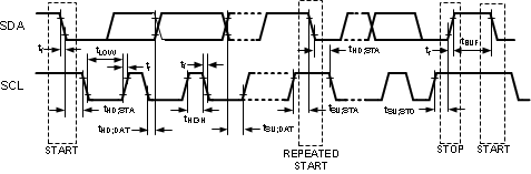 Figure 1. Serial Control Bus Timing
6.8 Serial Control Bus DC Characteristics (SCL, SDA) - I2C Compliant
Over recommended supply and temperature ranges unless otherwise specified.| PARAMETER | TEST CONDITIONS | MIN | TYP | MAX | UNIT | |
|---|---|---|---|---|---|---|
| VIH | Input High Level | SDA and SCL | 0.7 x VDDIO |
VDDIO | V | |
| VIL | Input Low Level Voltage | SDA and SCL | GND | 0.3 x VDDIO |
V | |
| VHY | Input Hysteresis | SDA and SCL | >50 | mV | ||
| IOZ | TRI-STATE Output Current | PDB = 0V VOUT = 0V or VDD |
-20 | ±1 | +20 | µA |
| IIN | Input Current | SDA or SCL, Vin = VDDIO or GND |
-20 | ±1 | +20 | µA |
| CIN | Input Pin Capacitance | <5 | pF | |||
| VOL | Low Level Output Voltage | SCL and SDA VDDIO = 3.0V IOL = 1.5mA |
0.36 | V | ||
| SCL and SDA VDDIO = 1.71V IOL = 1mA |
0.36 | V |
(1) “Absolute Maximum Ratings” indicate limits beyond which damage to the device may occur, including inoperability and degradation of device reliability and/or performance. Functional operation of the device and/or non-degradation at the Absolute Maximum Ratings or other conditions beyond those indicated in the Recommended Operating Conditions is not implied. The Recommended Operating Conditions indicate conditions at which the device is functional; the device should not be operated beyond such conditions.
(2) If Military/Aerospace specified devices are required, please contact the Texas Instruments Sales Office/ Distributors for availability and specifications.
(3) The Electrical Characteristics tables list ensured specifications under the listed Recommended Operating Conditions except as otherwise modified or specified by the Electrical Characteristics Conditions and/or Notes. Typical specifications are estimations only and are not ensured.
(4) Current into device pins is defined as positive. Current out of a device pin is defined as negative. Voltages are referenced to ground except VOD, ΔVOD, VTH and VTL which are differential voltages.
(5) Typical values represent most likely parametric norms at 1.8V or 3.3V, TA = +25°C, and at the Recommended Operation Conditions at the time of product characterization and are not ensured.
(6) tPLD and tDDLT is the time required by the serializer and deserializer to obtain lock when exiting power-down state with an active PCLK
(7) tDCJ is the maximum amount of jitter measured over 30,000 samples based on Time Interval Error (TIE).
(8) tDPJ is the maximum amount the period is allowed to deviate measured over 30,000 samples.
(9) tDCCJ is the maximum amount of jitter between adjacent clock cycles measured over 30,000 samples.
(10) Specification is ensured by characterization and is not tested in production.
(11) Specification is ensured by design.
(12) Recommended Input Timing Requirements are input specifications and not tested in production.
(13) UI – Unit Interval is equivalent to one ideal serialized data bit width. The UI scales with PCLK frequency.
(14) tRJIT max (0.61UI) is limited by instrumentation and actual tRJIT of in-band jitter at low frequency (<2 MHz) is greater 1 UI.
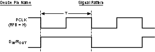 Figure 2. “Worst Case” Test Pattern
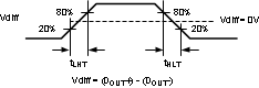 Figure 3. Serializer CML Output Load and Transition Times
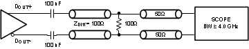 Figure 4. Serializer CML Output Load and Transition Times
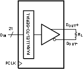 Figure 5. Serializer VOD DC Diagram
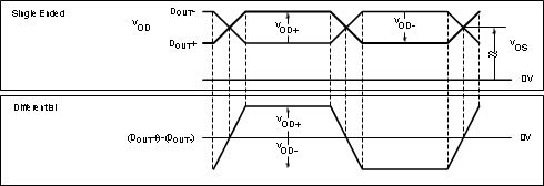 Figure 6. Serializer VOD DC Diagram
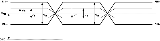 Figure 7. Differential VTH/VTL Definition Diagram
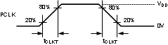 Figure 8. Serializer Input Clock Transition Times
 Figure 9. Serializer Setup/Hold Times
 Figure 10. Serializer Data Lock Time
 Figure 11. Serializer Delay
 Figure 12. Deserializer Data Lock Time
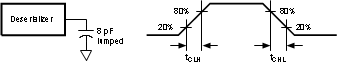 Figure 13. Deserializer LVCMOS Output Load and Transition Times
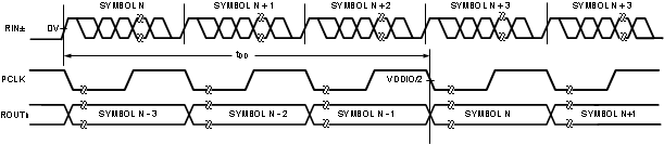 Figure 14. Deserializer Delay
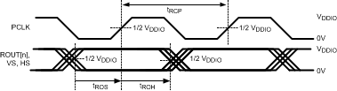 Figure 15. Deserializer Output Setup/Hold Times
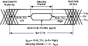 Figure 16. Receiver Input Jitter Tolerance
 Figure 17. Spread Spectrum Clock Output Profile
6.9 Serializer Switching Characteristics
Over recommended operating supply and temperature ranges unless otherwise specified.| PARAMETER | TEST CONDITIONS | MIN | TYP | MAX | UNIT | |
|---|---|---|---|---|---|---|
| tLHT | CML Low-to-High Transition Time | RL = 100Ω Figure 3 |
150 | 330 | ps | |
| tHLT | CML High-to-Low Transition Time | RL = 100Ω Figure 3 |
150 | 330 | ps | |
| tDIS | Data Input Setup to PCLK | Serializer Data Inputs Figure 9 |
2.0 | ns | ||
| tDIH | Data Input Hold from PCLK | 2.0 | ns | |||
| tPLD | Serializer PLL Lock Time | RL = 100Ω(6)(11) | 1 | 2 | ms | |
| tSD | Serializer Delay | RT = 100Ω PCLK = 10–43 MHz Register 0x03h b[0] (TRFB = 1) Figure 11 |
6.386T + 5 |
6.386T + 12 |
6.386T + 19.7 |
ns |
| tJIND | Serializer Output Deterministic Jitter | Serializer output intrinsic deterministic jitter . Measured (cycle-cycle) with PRBS-7 test pattern PCLK = 43 MHz(5)(13) |
0.13 | UI | ||
| tJINR | Serializer Output Random Jitter | Serializer output intrinsic random jitter (cycle-cycle). Alternating-1,0 pattern. PCLK = 43 MHz(5)(13) |
0.04 | UI | ||
| tJINT | Peak-to-peak Serializer Output Jitter | Serializer output peak-to-peak jitter includes deterministic jitter, random jitter, and jitter transfer from serializer input. Measured (cycle-cycle) with PRBS-7 test pattern. PCLK = 43 MHz(5)(13) |
0.396 | UI | ||
| λSTXBW | Serializer Jitter Transfer Function -3 dB Bandwidth | PCLK = 43 MHz Default Registers Figure 18(5) |
1.90 | MHz | ||
| δSTX | Serializer Jitter Transfer Function (Peaking) | PCLK = 43 MHz Default Registers Figure 18(5) |
0.944 | dB | ||
| δSTXf | Serializer Jitter Transfer Function (Peaking Frequency) | PCLK = 43 MHz Default Registers Figure 18(5) |
500 | kHz |
6.10 Deserializer Switching Characteristics
Over recommended operating supply and temperature ranges unless otherwise specified.| PARAMETER | TEST CONDITIONS | PIN/FREQ. | MIN | TYP | MAX | UNIT | |
|---|---|---|---|---|---|---|---|
| tRCP | Receiver Output Clock Period | tRCP = tTCP | PCLK | 23.3 | T | 100 | ns |
| tPDC | PCLK Duty Cycle | Default Registers SSCG[3:0] = OFF |
PCLK | 45 | 50 | 55 | % |
| tCLH | LVCMOS Low-to-High Transition Time | VDDIO: 1.71V to 1.89V or 3.0 to 3.6V, CL = 8 pF (lumped load) Default Registers Figure 13(10) |
PCLK | 1.3 | 2.0 | 2.8 | ns |
| tCHL | LVCMOS High-to-Low Transition Time | 1.3 | 2.0 | 2.8 | |||
| tCLH | LVCMOS Low-to-High Transition Time | VDDIO: 1.71V to 1.89V or 3.0 to 3.6V, CL = 8 pF (lumped load) Default Registers Figure 13(10) |
Deserializer ROUTn Data Outputs | 1.6 | 2.4 | 3.3 | ns |
| tCHL | LVCMOS High-to-Low Transition Time | 1.6 | 2.4 | 3.3 | |||
| tROS | ROUT Setup Data to PCLK |
VDDIO: 1.71V to 1.89V or 3.0V to 3.6V, CL = 8 pF (lumped load) Default Registers |
Deserializer ROUTn Data Outputs | 0.38T | 0.5T | ns | |
| tROH | ROUT Hold Data to PCLK | 0.38T | 0.5T | ||||
| tDD | Deserializer Delay | Default Registers Register 0x03h b[0] (RRFB = 1) Figure 14 |
10 MHz–43 MHz | 4.571T + 8 |
4.571T + 12 |
4.571T + 16 |
ns |
| tDDLT | Deserializer Data Lock Time | Figure 12(6) | 10 MHz–43 MHz | 10 | ms | ||
| tRJIT | Receiver Input Jitter Tolerance | Figure 16, Figure 19(13)(14) | 43 MHz | 0.53 | UI | ||
| tRCJ | Receiver Clock Jitter | PCLK SSCG[3:0] = OFF(10)(7) |
10 MHz | 300 | 550 | ps | |
| 43 MHz | 120 | 250 | |||||
| tDPJ | Deserializer Period Jitter | PCLK SSCG[3:0] = OFF (10)(8) |
10 MHz | 425 | 600 | ps | |
| 43 MHz | 320 | 480 | |||||
| tDCCJ | Deserializer Cycle-to-Cycle Clock Jitter | PCLK SSCG[3:0] = OFF(10)(9) |
10 MHz | 320 | 500 | ps | |
| 43 MHz | 300 | 500 | |||||
| fdev | Spread Spectrum Clocking Deviation Frequency | LVCMOS Output Bus SSC[3:0] = ON Figure 17 |
20 MHz–43 MHz | ±0.5% to ±2.0% | % | ||
| fmod | Spread Spectrum Clocking Modulation Frequency | 20 MHz–43 MHz | 9 kHz to 66 kHz | kHz |
6.11 Typical Characteristics
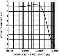
Transfer Function Curve at 43 MHz
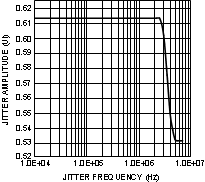
Tolerance Curve at 43 MHz