SNLS346C August 2011 – June 2014 DS90UR903Q-Q1 , DS90UR904Q-Q1
PRODUCTION DATA.
- 1 Features
- 2 Applications
- 3 Description
- 4 Revision History
- 5 Pin Configuration and Functions
-
6 Specifications
- 6.1 Absolute Maximum Ratings
- 6.2 Handling Ratings
- 6.3 Recommended Operating Conditions
- 6.4 Thermal Information
- 6.5 Electrical Characteristics
- 6.6 Recommended Serializer Timing for PCLK
- 6.7 Serial Control Bus AC Timing Specifications (SCL, SDA) - I2C Compliant (See )
- 6.8 Serial Control Bus DC Characteristics (SCL, SDA) - I2C Compliant
- 6.9 Serializer Switching Characteristics
- 6.10 Deserializer Switching Characteristics
- 6.11 Typical Characteristics
- 7 Detailed Description
- 8 Application and Implementation
- 9 Power Supply Recommendations
- 10Layout
- 11Device and Documentation Support
- 12Mechanical, Packaging, and Orderable Information
Package Options
Mechanical Data (Package|Pins)
- RHS|48
Thermal pad, mechanical data (Package|Pins)
- RHS|48
Orderable Information
5 Pin Configuration and Functions
40 Pin Serializer – DS90UR903Q
Package RTA
Top View
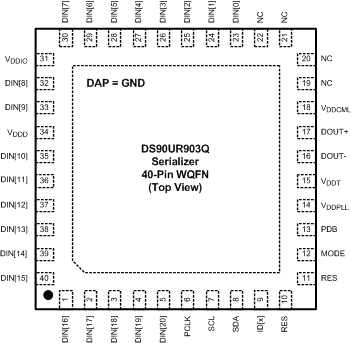
DS90UR903Q Serializer Pin Functions
| PIN | I/O, TYPE | DESCRIPTION | |
|---|---|---|---|
| NAME | NUMBER | ||
| LVCMOS PARALLEL INTERFACE | |||
| DIN[20:0] | 5, 4, 3, 2, 1, 40, 39, 38, 37, 36, 35, 33, 32, 30, 29, 28, 27, 26, 25, 24, 23 | Inputs, LVCMOS w/ pull down |
Parallel data inputs. |
| PCLK | 6 | Input, LVCMOS w/ pull down |
Pixel Clock Input Pin. Strobe edge set by TRFB control register. |
| SERIAL CONTROL BUS - I2C COMPATIBLE | |||
| SCL | 7 | Input, Open Drain |
Clock line for the serial control bus communication SCL requires an external pull-up resistor to VDDIO. |
| SDA | 8 | Input/Output, Open Drain |
Data line for the serial control bus communication SDA requires an external pull-up resistor to VDDIO. |
| MODE | 12 | Input, LVCMOS w/ pull down |
I2C Mode select MODE = H, -REQUIRED. The MODE pin must be set HIGH to allow I2C configuration of the serializer. |
| ID[x] | 9 | Input, analog | Device ID Address Select Resistor to Ground and 10 kΩ pull-up to 1.8V rail. See Table 1 |
| CONTROL AND CONFIGURATION | |||
| PDB | 13 | Input, LVCMOS w/ pull down |
Power down Mode Input Pin. PDB = H, Serializer is enabled and is ON. PDB = L, Serailizer is in Power Down mode. When the Serializer is in Power Down, the PLL is shutdown, and IDD is minimized. Programmed control register data are NOT retained and reset to default values |
| RES | 10, 11 | Input, LVCMOS w/ pull down |
Reserved. This pin MUST be tied LOW. |
| NC | 22, 21, 20, 19 | No Connect | |
| FPD-LINK II INTERFACE | |||
| DOUT+ | 17 | Output, CML | Non-inverting differential output. The interconnect must be AC Coupled with a 100 nF capacitor. |
| DOUT- | 16 | Output, CML | Inverting differential output. The interconnect must be AC Coupled with a 100 nF capacitor. |
| POWER AND GROUND(1) | |||
| VDDPLL | 14 | Power, Analog | PLL Power, 1.8V ±5% |
| VDDT | 15 | Power, Analog | Tx Analog Power, 1.8V ±5% |
| VDDCML | 18 | Power, Analog | CML Power, 1.8V ±5% |
| VDDD | 34 | Power, Digital | Digital Power, 1.8V ±5% |
| VDDIO | 31 | Power, Digital | Power for I/O stage. The single-ended inputs and SDA, SCL are powered from VDDIO. VDDIO can be connected to a 1.8V ±5% or 3.3V ±10% |
| VSS | DAP | Ground, DAP | DAP must be grounded. DAP is the large metal contact at the bottom side, located at the center of the WQFN package. Connected to the ground plane (GND) with at least 16 vias. |
(1) See Power Up Requirements and PDB PIN.
48 Pin Deserializer - DS90UR904Q
Package RHS
Top View
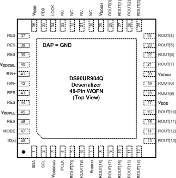
DS90UR904Q Deserializer Pin Descriptions
| PIN | I/O, TYPE | DESCRIPTION | |
|---|---|---|---|
| NAME | NUMBER | ||
| LVCMOS PARALLEL INTERFACE | |||
| ROUT[20:0] | 5, 6, 8, 9, 10, 11, 12, 13, 14, 15, 16, 18, 19, 21, 22, 23, 24, 25, 26, 27, 28 | Outputs, LVCMOS | Parallel data outputs. |
| PCLK | 4 | Output, LVCMOS | Pixel Clock Output Pin. Strobe edge set by RRFB control register. |
| SERIAL CONTROL BUS - I2C COMPATIBLE | |||
| SCL | 2 | Input, Open Drain |
Clock line for the serial control bus communication SCL requires an external pull-up resistor to VDDIO. |
| SDA | 1 | Input/Output, Open Drain |
Data line for the serial control bus communication SDA requires an external pull-up resistor to VDDIO. |
| MODE | 47 | Input, LVCMOS w/ pull up |
I2C Mode select MODE = H -REQUIRED. The MODE pin must be set HIGH to allow I2C configuration of the deserializer. |
| ID[x] | 9 | Input, analog | Device ID Address Select Resistor to Ground and 10 kΩ pull-up to 1.8V rail. See Table 2 |
| CONTROL AND CONFIGURATION | |||
| PDB | 35 | Input, LVCMOS w/ pull down |
Power down Mode Input Pin. PDB = H, Deserializer is enabled and is ON. PDB = L, Deserializer is in Power Down mode. When the Deserializer is in Power Down. Programmed control register data are NOT retained and reset to default values. |
| LOCK | 34 | Output, LVCMOS |
LOCK Status Output Pin. LOCK = H, PLL is Locked, outputs are active LOCK = L, PLL is unlocked, ROUT and PCLK output states are controlled by OSS_SEL control register. May be used as Link Status. |
| RES | 37, 38, 39, 43, 44, 46 | - | Reserved. Pin 46: This pin MUST be tied LOW. Pin 37, 43, 44: Leave pin open. Pins 38, 39: Route to test point or leave open if unused. |
| NC | 30, 31, 32, 33 | No Connect | |
| FPD-LINK II INTERFACE | |||
| RIN+ | 41 | Input, CML | Noninverting differential input. The interconnect must be AC Coupled with a 100 nF capacitor. |
| RIN- | 42 | Inputt, CML | Inverting differential input. The interconnect must be AC Coupled with a 100 nF capacitor. |
| POWER AND GROUND (1) | |||
| VDDSSCG | 3 | Power, Digital | SSCG Power, 1.8V ±5% Power supply must be connected regardless if SSCG function is in operation. |
| VDDIO1/2/3 | 29, 20, 7 | Power, Digital | LVCMOS I/O Buffer Power, The single-ended outputs and control input are powered from VDDIO. VDDIO can be connected to a 1.8V ±5% or 3.3V ±10% |
| VDDD | 17 | Power, Digital | Digital Core Power, 1.8V ±5% |
| VDDR | 36 | Power, Analog | Rx Analog Power, 1.8V ±5% |
| VDDCML | 40 | Power, Analog | 1.8V ±5% |
| VDDPLL | 45 | Power, Analog | PLL Power, 1.8V ±5% |
| VSS | DAP | Ground, DAP | DAP must be grounded. DAP is the large metal contact at the bottom side, located at the center of the WQFN package. Connected to the ground plane (GND) with at least 16 vias. |
(1) See Power Up Requirements and PDB PIN.