SNVS252H September 2003 – November 2018 LM5007
PRODUCTION DATA.
- 1 Features
- 2 Applications
- 3 Description
- 4 Revision History
- 5 Pin Configuration and Functions
- 6 Specifications
- 7 Detailed Description
-
8 Application and Implementation
- 8.1 Application Information
- 8.2
Typical Application
- 8.2.1 Design Requirements
- 8.2.2
Detailed Design Procedure
- 8.2.2.1 Custom Design With WEBENCH® Tools
- 8.2.2.2 Custom Design With Excel Quickstart Tool
- 8.2.2.3 Feedback Resistors, RFB1 and RFB2
- 8.2.2.4 Switching Frequency Selection, RON
- 8.2.2.5 Buck Inductor, L1
- 8.2.2.6 Output Capacitor, COUT
- 8.2.2.7 Type I Ripple Circuit, RC
- 8.2.2.8 Input Capacitor, CIN
- 8.2.2.9 Current Limit, RCL
- 8.2.3 Application Curves
- 9 Power Supply Recommendations
- 10Layout
- 11Device and Documentation Support
- 12Mechanical, Packaging, and Orderable Information
Package Options
Mechanical Data (Package|Pins)
Thermal pad, mechanical data (Package|Pins)
Orderable Information
7.3.2 High-Voltage Bias Supply Regulator
The LM5007 contains an internal high-voltage bias supply regulator. The input pin (VIN) can be connected directly to line voltages from 9 V to 75 V. To avoid supply voltage transients due to long lead inductances on the input pin (VIN), it is always recommended to connect a low-ESR ceramic capacitor (≈ 0.1 µF) between VIN and RTN, located close to the respective pins of the LM5007. The bias regulator is internally current limited to 10 mA. Upon power up, the regulator is enabled and sources current into an external capacitor connected to the VCC pin. When the VCC voltage reaches the regulation point of 7 V, the controller output is enabled.
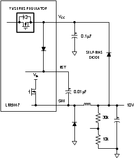
An external auxiliary supply voltage can be applied to the VCC pin. If this auxiliary voltage is greater than 7 V, the internal regulator will essentially shutoff, thus reducing internal power dissipation.
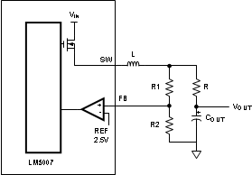
 Figure 4. Low Output Ripple Voltage Configuration
  Figure 5. Self-Biased Configuration with VOUT Feeding VCC Through a Diode