SNVS252H September 2003 – November 2018 LM5007
PRODUCTION DATA.
- 1 Features
- 2 Applications
- 3 Description
- 4 Revision History
- 5 Pin Configuration and Functions
- 6 Specifications
- 7 Detailed Description
-
8 Application and Implementation
- 8.1 Application Information
- 8.2
Typical Application
- 8.2.1 Design Requirements
- 8.2.2
Detailed Design Procedure
- 8.2.2.1 Custom Design With WEBENCH® Tools
- 8.2.2.2 Custom Design With Excel Quickstart Tool
- 8.2.2.3 Feedback Resistors, RFB1 and RFB2
- 8.2.2.4 Switching Frequency Selection, RON
- 8.2.2.5 Buck Inductor, L1
- 8.2.2.6 Output Capacitor, COUT
- 8.2.2.7 Type I Ripple Circuit, RC
- 8.2.2.8 Input Capacitor, CIN
- 8.2.2.9 Current Limit, RCL
- 8.2.3 Application Curves
- 9 Power Supply Recommendations
- 10Layout
- 11Device and Documentation Support
- 12Mechanical, Packaging, and Orderable Information
Package Options
Mechanical Data (Package|Pins)
Thermal pad, mechanical data (Package|Pins)
Orderable Information
7.3.4 On-Time Generator and Shutdown
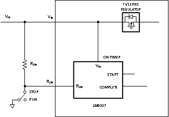
The on-time of the LM5007 is set inversely proportional to the input voltage by an external resistor connected between VIN and RON. The RON pin is a low impedance input biased at approximately 1.5 V. Thus, the current through the resistor and into the RON pin is approximately proportional to VIN and used internally to control the on-timer. This scheme of input voltage feedforward hysteretic operation achieves nearly constant switching frequency over varying line and load conditions. Equation 4 specifies the on-time equation for the LM5007.

The RON pin of the LM5007 also provides a shutdown function that disables the converter and significantly decreases quiescent power dissipation. Pulling the voltage at RON below a 0.7-V logic threshold activates a low-power shutdown mode. The VIN quiescent current in this shutdown mode is approximately 100 µA internal to the LM5007 plus the current in the RON resistor.
 Figure 6. Shutdown Implementation