SNVSB54A May 2018 – November 2018 LM5122ZA
PRODUCTION DATA.
- 1 Features
- 2 Applications
- 3 Description
- 4 Revision History
- 5 Pin Configuration and Functions
- 6 Specifications
-
7 Detailed Description
- 7.1 Overview
- 7.2 Functional Block Diagram
- 7.3
Feature Description
- 7.3.1 Undervoltage Lockout (UVLO)
- 7.3.2 High-Voltage VCC Regulator
- 7.3.3 Oscillator
- 7.3.4 Slope Compensation
- 7.3.5 Error Amplifier
- 7.3.6 PWM Comparator
- 7.3.7 Soft Start
- 7.3.8 HO and LO Drivers
- 7.3.9 Bypass Operation (VOUT = VIN)
- 7.3.10 Cycle-by-Cycle Current Limit
- 7.3.11 Clock Synchronization
- 7.3.12 Maximum Duty Cycle
- 7.3.13 Thermal Protection
- 7.4 Device Functional Modes
-
8 Application and Implementation
- 8.1
Application Information
- 8.1.1 Feedback Compensation
- 8.1.2 Sub-Harmonic Oscillation
- 8.1.3 Interleaved Boost Configuration
- 8.1.4 DCR Sensing
- 8.1.5 Output Overvoltage Protection
- 8.1.6 SEPIC Converter Simplified Schematic
- 8.1.7 Non-Isolated Synchronous Flyback Converter Simplified Schematic
- 8.1.8 Negative to Positive Conversion
- 8.2
Typical Application
- 8.2.1 Design Requirements
- 8.2.2
Detailed Design Procedure
- 8.2.2.1 Timing Resistor RT
- 8.2.2.2 UVLO Divider RUV2, RUV1
- 8.2.2.3 Input Inductor LIN
- 8.2.2.4 Current Sense Resistor RS
- 8.2.2.5 Current Sense Filter RCSFP, RCSFN, CCS
- 8.2.2.6 Slope Compensation Resistor RSLOPE
- 8.2.2.7 Output Capacitor COUT
- 8.2.2.8 Input Capacitor CIN
- 8.2.2.9 VIN Filter RVIN, CVIN
- 8.2.2.10 Bootstrap Capacitor CBST and Boost Diode DBST
- 8.2.2.11 VCC Capacitor CVCC
- 8.2.2.12 Output Voltage Divider RFB1, RFB2
- 8.2.2.13 Soft-Start Capacitor CSS
- 8.2.2.14 Restart Capacitor CRES
- 8.2.2.15 Low-Side Power Switch QL
- 8.2.2.16 High-Side Power Switch QH and Additional Parallel Schottky Diode
- 8.2.2.17 Snubber Components
- 8.2.2.18 Loop Compensation Components CCOMP, RCOMP, CHF
- 8.2.3 Application Curves
- 8.1
Application Information
- 9 Power Supply Recommendations
- 10Layout
- 11Device and Documentation Support
- 12Mechanical, Packaging, and Orderable Information
Package Options
Refer to the PDF data sheet for device specific package drawings
Mechanical Data (Package|Pins)
- PWP|24
Thermal pad, mechanical data (Package|Pins)
Orderable Information
7.3.2 High-Voltage VCC Regulator
The LM5122ZA contains an internal high-voltage regulator that provides typical 7.6 V VCC bias supply for the controller and N-channel MOSFET drivers. The input of VCC regulator, VIN, can be connected to an input voltage source as high as 65 V. The VCC regulator turns on when the UVLO pin voltage is greater than 0.4 V. When the input voltage is below the VCC setpoint level, the VCC output tracks VIN with a small dropout voltage. The output of the VCC regulator is current limited at 50 mA minimum.
Upon power up, the VCC regulator sources current into the capacitor connected to the VCC pin. TI recommends a capacitance range for the VCC capacitor of 1 μF to 47 μF; capacitance at least 10 times greater than CBST value is also recommnded. When operating with a VIN voltage less than 6 V, the value of VCC capacitor must be 4.7 µF or greater.
The internal power dissipation of the LM5122ZA device can be reduced by supplying VCC from an external supply. If an external VCC bias supply exists and the voltage is greater than 9 V and below 14.5 V. The external VCC bias supply can be applied to the VCC pin directly through a diode, as shown in Figure 17.
 Figure 17. External Bias Supply when 9 V < VEXT< 14.5 V
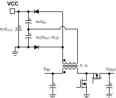
 A method to derive the VCC bias voltage with an additional winding on the boost inductor is shown in . This circuit must be designed to raise the VCC voltage above VCC regulation voltage to shut off the internal VCC regulator.
 Figure 18. External Bias Supply using Transformer
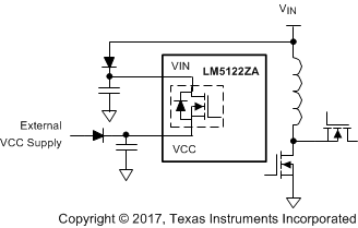
 The VCC regulator series pass transistor includes a diode between VCC and VIN that must not be fully forward biased in normal operation, as shown in Figure 19. If the voltage of the external VCC bias supply is greater than the VIN pin voltage, an external blocking diode is required from the input power supply to the VIN pin to prevent the external bias supply from passing current to the input supply through VCC. The need for the blocking diode should be evaluated for all applications when the VCC is supplied by the external bias supply. Especially, when the input power supply voltage is less than 4.5 V, the external VCC supply should be provided and the external blocking diode is required.
 Figure 19. VIN Configuration when VVIN < VVCC