SNVSB54A May 2018 – November 2018 LM5122ZA
PRODUCTION DATA.
- 1 Features
- 2 Applications
- 3 Description
- 4 Revision History
- 5 Pin Configuration and Functions
- 6 Specifications
-
7 Detailed Description
- 7.1 Overview
- 7.2 Functional Block Diagram
- 7.3
Feature Description
- 7.3.1 Undervoltage Lockout (UVLO)
- 7.3.2 High-Voltage VCC Regulator
- 7.3.3 Oscillator
- 7.3.4 Slope Compensation
- 7.3.5 Error Amplifier
- 7.3.6 PWM Comparator
- 7.3.7 Soft Start
- 7.3.8 HO and LO Drivers
- 7.3.9 Bypass Operation (VOUT = VIN)
- 7.3.10 Cycle-by-Cycle Current Limit
- 7.3.11 Clock Synchronization
- 7.3.12 Maximum Duty Cycle
- 7.3.13 Thermal Protection
- 7.4 Device Functional Modes
-
8 Application and Implementation
- 8.1
Application Information
- 8.1.1 Feedback Compensation
- 8.1.2 Sub-Harmonic Oscillation
- 8.1.3 Interleaved Boost Configuration
- 8.1.4 DCR Sensing
- 8.1.5 Output Overvoltage Protection
- 8.1.6 SEPIC Converter Simplified Schematic
- 8.1.7 Non-Isolated Synchronous Flyback Converter Simplified Schematic
- 8.1.8 Negative to Positive Conversion
- 8.2
Typical Application
- 8.2.1 Design Requirements
- 8.2.2
Detailed Design Procedure
- 8.2.2.1 Timing Resistor RT
- 8.2.2.2 UVLO Divider RUV2, RUV1
- 8.2.2.3 Input Inductor LIN
- 8.2.2.4 Current Sense Resistor RS
- 8.2.2.5 Current Sense Filter RCSFP, RCSFN, CCS
- 8.2.2.6 Slope Compensation Resistor RSLOPE
- 8.2.2.7 Output Capacitor COUT
- 8.2.2.8 Input Capacitor CIN
- 8.2.2.9 VIN Filter RVIN, CVIN
- 8.2.2.10 Bootstrap Capacitor CBST and Boost Diode DBST
- 8.2.2.11 VCC Capacitor CVCC
- 8.2.2.12 Output Voltage Divider RFB1, RFB2
- 8.2.2.13 Soft-Start Capacitor CSS
- 8.2.2.14 Restart Capacitor CRES
- 8.2.2.15 Low-Side Power Switch QL
- 8.2.2.16 High-Side Power Switch QH and Additional Parallel Schottky Diode
- 8.2.2.17 Snubber Components
- 8.2.2.18 Loop Compensation Components CCOMP, RCOMP, CHF
- 8.2.3 Application Curves
- 8.1
Application Information
- 9 Power Supply Recommendations
- 10Layout
- 11Device and Documentation Support
- 12Mechanical, Packaging, and Orderable Information
Package Options
Refer to the PDF data sheet for device specific package drawings
Mechanical Data (Package|Pins)
- PWP|24
Thermal pad, mechanical data (Package|Pins)
Orderable Information
8.1.2 Sub-Harmonic Oscillation
Peak current mode regulator can exhibit unstable behavior when operating above 50% duty cycle. This behavior is known as sub-harmonic oscillation and is characterized by alternating wide and narrow pulses at the SW pin. Sub-harmonic oscillation can be prevented by adding an additional slope voltage ramp (slope compensation) on top of the sensed inductor current. By choosing K ≥ 0.82~1, the sub-harmonic oscillation is eliminated even with wide varying input voltage.
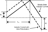
In time-domain analysis, the steady-state inductor current starting from an initial point returns to the same point. When the amplitude of an end cycle current error (dI1) caused by an initial perturbation (dI0) is less than the amplitude of dI0 or dI1/dI0 > –1, the perturbation naturally disappears after a few cycles. When dl1/dl0 < –1, the initial perturbation no longer disappear, it results in sub-harmonic oscillation in steady-state.
 Figure 27. Effect of Initial Perturbation when dl1/dl0 < –1
 dI1/dI0 can be calculated as:

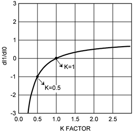
The relationship between dI1/dI0 and K factor is illustrated graphically in Figure 28.
 Figure 28. dl1/dl0 vs K Factor
 The absolute minimum value of K is 0.5. When K < 0.5, the amplitude of dl1 is greater than the amplitude of dl0 and any initial perturbation results in sub-harmonic oscillation. If K = 1, any initial perturbation is removed in one switching cycle. This is known as one-cycle damping. When –1 < dl1/dl0 < 0, any initial perturbationis under-damped. Any perturbation is over-damped when 0 < dl1/dl0 < 1.
In the frequency-domain, Q, the quality factor of sampling gain term in modulator transfer function, is used to predict the tendency for sub-harmonic oscillation, which is defined as:

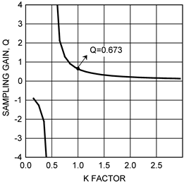
The relationship between Q and K factor is shown in Figure 29.
 Figure 29. Sampling Gain Q vs K Factor
 The recommended absolute minimum value of K is 0.5. High gain peaking when K is less than 0.5 results sub-harmonic oscillation at fSW/2. A higher value of K factor may introduce additional phase shift near the crossover frequency, but has the benefit of reducing noise susceptibility in current loop. The maximum allowable value of K factor can be calculated by the maximum crossover frequency equation in frequency analysis formulas in Table 2.
Table 2. Boost Regulator Frequency Analysis
| SIMPLIFIED FORMULA | COMPREHENSIVE FORMULA(1) | |
|---|---|---|
| MODULATOR TRANSER FUNCTION |
 |
 |
| Modulator DC gain (2) |
 |
|
| RHP zero (2) |
 |
|
| ESR zero |
 |
 |
| ESR pole | Not considered |
 |
| Dominant load pole |
 |
|
| Sampled gain inductor pole | Not considered |
  |
| Quality factor | Not considered |
 |
| Sub-harmonic double pole | Not considered |
 or  |
| K factor | K = 1 |
 |
| FEEDBACK TRANSFER FUNCTION |
 |
|
| Feedback DC gain |
 |
|
| Mid-band Gain |
 |
|
| Low frequency zero |
 |
|
| High frequency pole |
 |
 |
| OPEN LOOP RESPONSE |
 |
 |
| Crossover frequency (3)
(Open loop band width) |
 |
Use graphic tool |
| Maximum cross over frequency(4) |
 |
  |
 ,
,  ,
,  , and COUT = COUT of each phase x n, where n = number of phases. As is the current sense amplifier gain.
  ,
,  ,
,  ,
,  , and
, and  .
.