SNVSB54A May 2018 – November 2018 LM5122ZA
PRODUCTION DATA.
- 1 Features
- 2 Applications
- 3 Description
- 4 Revision History
- 5 Pin Configuration and Functions
- 6 Specifications
-
7 Detailed Description
- 7.1 Overview
- 7.2 Functional Block Diagram
- 7.3
Feature Description
- 7.3.1 Undervoltage Lockout (UVLO)
- 7.3.2 High-Voltage VCC Regulator
- 7.3.3 Oscillator
- 7.3.4 Slope Compensation
- 7.3.5 Error Amplifier
- 7.3.6 PWM Comparator
- 7.3.7 Soft Start
- 7.3.8 HO and LO Drivers
- 7.3.9 Bypass Operation (VOUT = VIN)
- 7.3.10 Cycle-by-Cycle Current Limit
- 7.3.11 Clock Synchronization
- 7.3.12 Maximum Duty Cycle
- 7.3.13 Thermal Protection
- 7.4 Device Functional Modes
-
8 Application and Implementation
- 8.1
Application Information
- 8.1.1 Feedback Compensation
- 8.1.2 Sub-Harmonic Oscillation
- 8.1.3 Interleaved Boost Configuration
- 8.1.4 DCR Sensing
- 8.1.5 Output Overvoltage Protection
- 8.1.6 SEPIC Converter Simplified Schematic
- 8.1.7 Non-Isolated Synchronous Flyback Converter Simplified Schematic
- 8.1.8 Negative to Positive Conversion
- 8.2
Typical Application
- 8.2.1 Design Requirements
- 8.2.2
Detailed Design Procedure
- 8.2.2.1 Timing Resistor RT
- 8.2.2.2 UVLO Divider RUV2, RUV1
- 8.2.2.3 Input Inductor LIN
- 8.2.2.4 Current Sense Resistor RS
- 8.2.2.5 Current Sense Filter RCSFP, RCSFN, CCS
- 8.2.2.6 Slope Compensation Resistor RSLOPE
- 8.2.2.7 Output Capacitor COUT
- 8.2.2.8 Input Capacitor CIN
- 8.2.2.9 VIN Filter RVIN, CVIN
- 8.2.2.10 Bootstrap Capacitor CBST and Boost Diode DBST
- 8.2.2.11 VCC Capacitor CVCC
- 8.2.2.12 Output Voltage Divider RFB1, RFB2
- 8.2.2.13 Soft-Start Capacitor CSS
- 8.2.2.14 Restart Capacitor CRES
- 8.2.2.15 Low-Side Power Switch QL
- 8.2.2.16 High-Side Power Switch QH and Additional Parallel Schottky Diode
- 8.2.2.17 Snubber Components
- 8.2.2.18 Loop Compensation Components CCOMP, RCOMP, CHF
- 8.2.3 Application Curves
- 8.1
Application Information
- 9 Power Supply Recommendations
- 10Layout
- 11Device and Documentation Support
- 12Mechanical, Packaging, and Orderable Information
Package Options
Refer to the PDF data sheet for device specific package drawings
Mechanical Data (Package|Pins)
- PWP|24
Thermal pad, mechanical data (Package|Pins)
Orderable Information
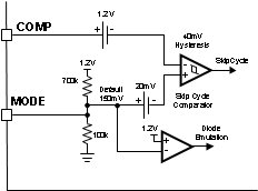
7.4.1 MODE Control (Forced-PWM Mode and Diode-Emulation Mode)
A fully synchronous boost regulator implemented with a high-side switch rather than a diode has the capability to sink current from the output in certain conditions such as light load, overvoltage, or load transient. The LM5122ZA can be configured to operate in either forced-PWM mode (FPWM) or diode emulation mode.
In FPWM, reverse current flow in high-side N-channel MOSFET switch is allowed, and the inductor current conducts continuously at light or no load conditions. The benefit of the FPWM mode is fast light load to heavy load transient response and constant frequency operation at light or no load conditions. To enable FPWM, connect the MODE pin to VCC or tie to a voltage greater than 1.2 V. In FPWM, reverse current flow is not limited.
In diode-emulation mode, current flow in the high-side switch is only permitted in one direction (source to drain). Turnon of the high-side switch is allowed if CSP to CSN voltage is greater than 7 mV rising threshold of zero current detection during low-side switch on-time. If CSP to CSN voltage is less than 6-mV falling threshold of zero current detection during high-side switch on-time, reverse current flow from output to input through the high-side N-channel MOSFET switch is prevented and discontinuous conduction mode of operation is enabled by latching off the high-side N-channel MOSFET switch for the remainder of the PWM cycle. A benefit of the diode emulation is lower power loss at light load conditions.
 Figure 25. MODE Selection
 During start-up the LM5122ZA forces diode emulation, for start-up into a pre-biased load, while the SS pin voltage is less than 1.2 V. Forced diode emulation is terminated by a pulse from the PWM comparator when SS is greater than 1.2 V. If there are no LO pulses during the soft-start period, a 350-ns one-shot LO pulse is forced at the end of soft start to help charge the boot strap capacitor. Due to the internal current sense delay, configuring the LM5122ZA for diode emulation mode must be carefully evaluated if the inductor current ripple ratio is high and when operating at very high switching frequency. The transient performance during full load to no load in FPWM mode should also be verified.