SNCS103E November 2004 – August 2018 LMH6574
PRODUCTION DATA.
- 1 Features
- 2 Applications
- 3 Description
- 4 Revision History
- 5 Pin Configuration and Functions
- 6 Specifications
- 7 Detailed Description
- 8 Application and Implementation
- 9 Power Supply Recommendations
- 10Layout
- 11Device and Documentation Support
- 12Mechanical, Packaging, and Orderable Information
Package Options
Mechanical Data (Package|Pins)
- D|14
Thermal pad, mechanical data (Package|Pins)
- D|14
Orderable Information
8.1.1 Multiplexer Expansion
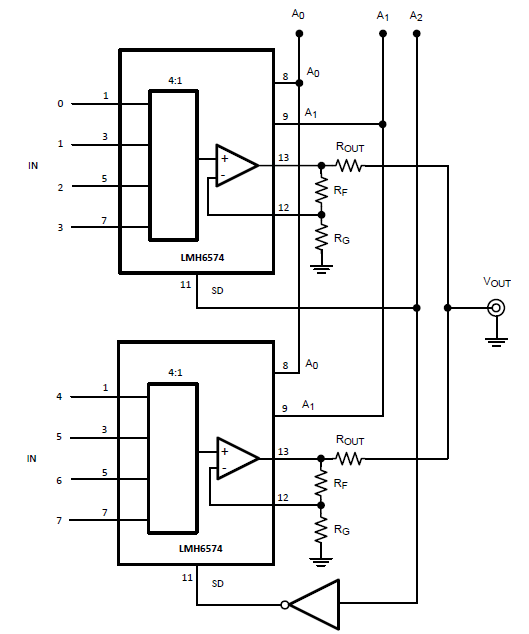
It is possible to use multiple LMH6574 devices to expand the number of inputs that can be selected for output. Figure 31 shows an 8:1 MUX using two LMH6574 devices.
 Figure 31. 8:1 MUX Using Two LMH6574 Devices
 In such an application, the output settling may be longer than the LMH6574 switching specifications (~20ns), while switching between two separate LMH6574 devices. The switching time limiting factor occurs when one LMH6574 is turned off and another one is turned on, using the SD (shutdown) pin. The output settling time consists of the time needed for the first LMH6574 to enter high impedance state plus the time required for the second LMH6574 output to dissipate the left-over output charge of the first device (limited by the output current capability of the second device) and the time needed to settle to the final voltage value.
While Figure 31 MUX expansion benefits from more isolation, originating from the parasitic loading of the un-selected channels on the selected channel, afforded by individual ROUT on each multiplexer output, this configuration does not produce the fastest transition between individual LMH6574 devices. For the fastest transition, the configuration of Figure 32 can be used where the LMH6574 output pins are all shorted together.
 Figure 32. Alternate 8:1 MUX Expansion Schematic (for Faster SD Switching)
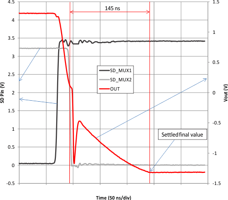
 Figure 33 shows typical transition waveforms and shows that SD pin switching settles in less than 145 ns.
 Figure 33. SD Pin Switching Waveform and Output Settling
 If it is important in the end application to make sure that no two inputs are presented to the output at the same time, an optional delay block can be added, to drive the SHUTDOWN pin of each device. Figure 34 shows one possible approach to this delay circuit. The delay circuit shown will delay SHUTDOWN's H to L transitions (R1 and C1 decay) but will not delay its L to H transition. R2 should be kept small compared to R1 in order to not reduce the SHUTDOWN voltage and to produce little or no delay to SHUTDOWN.
 Figure 34. Delay Circuit Implementation
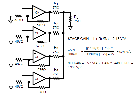
 With the SHUTDOWN pin putting the output stage into a high impedance state, several LMH6574’s can be tied together to form a larger input MUX. However, there is a loading effect on the active output caused by the unselected devices. The circuit in Figure 35 shows how to compensate for this effect. For the 16:1 MUX function shown in Figure 35, the gain error would be about −0.8 dB, or about 9%. In the circuit in Figure 35, resistor ratios have been adjusted to compensate for this gain error. By adjusting the gain of each multiplexer circuit the error can be reduced to the tolerance of the resistors used (1% in this example).
 Figure 35. Multiplexer Gain Compensation
 NOTE
Disabling of the LMH6574 using the EN pin is not recommended for use when doing multiplexer expansion. While disabled, If the voltage between the selected input and the chip output exceeds approximately 2V the device will begin to enter a soft breakdown state. This will show up as reduced input to output isolation. The signal on the non-inverting input of the output driver amplifier will leak through to the inverting input, and then to the output through the feedback resistor. The worst case is a gain of 1 configuration where the non inverting input follows the active input buffer and (through the feedback resistor) the inverting input follows the voltage driving the output stage. The solution for this is to use shutdown mode for multiplexer expansion.