SBOS567A June   2011  – February 2024 OPA564-Q1

PRODUCTION DATA  

  1.   1
  2. Features
  3. Applications
  4. Description
  5. Device Comparison Table
  6. Pin Configuration and Functions
  7. Specifications
    1. 6.1 Absolute Maximum Ratings
    2. 6.2 ESD Ratings
    3. 6.3 Recommended Operating Conditions
    4. 6.4 Thermal Information
    5. 6.5 Electrical Characteristics
    6. 6.6 Typical Characteristics
  8. Detailed Description
    1. 7.1 Overview
    2. 7.2 Functional Block Diagram
    3. 7.3 Feature Description
      1. 7.3.1 Adjustable Current Limit
        1. 7.3.1.1 Setting the Current Limit
      2. 7.3.2 Enable and Shutdown (E/S) Pin
      3. 7.3.3 Input Protection
      4. 7.3.4 Output Shutdown
      5. 7.3.5 Microcontroller Compatibility
      6. 7.3.6 Current Limit Flag
      7. 7.3.7 Thermal Protection
      8. 7.3.8 Junction Temperature Measurement Using TSENSE
    4. 7.4 Device Functional Modes
  9. Application and Implementation
    1. 8.1 Application Information
      1. 8.1.1 Basic Configuration
      2. 8.1.2 Output-Stage Compensation
      3. 8.1.3 Output Protection
      4. 8.1.4 Power Dissipation and Safe Operating Area
    2. 8.2 Typical Applications
      1. 8.2.1 Improved Howland Current Pump
      2. 8.2.2 Programmable Power Supply
      3. 8.2.3 Powerline Communication
      4. 8.2.4 Motor-Drive Circuit
      5. 8.2.5 DC Motor-Speed Controller (Without Tachometer)
      6. 8.2.6 Generating VDIG
      7. 8.2.7 Temperature Measurement
    3. 8.3 Power Supply Recommendations
    4. 8.4 Layout
      1. 8.4.1 Layout Guidelines
        1. 8.4.1.1 Thermally Enhanced PowerPAD™ Integrated Circuit Package
          1. 8.4.1.1.1 Bottom-Side Thermal Pad Assembly Process
  10. Device and Documentation Support
    1. 9.1 Receiving Notification of Documentation Updates
    2. 9.2 Support Resources
    3. 9.3 Trademarks
    4. 9.4 Electrostatic Discharge Caution
    5. 9.5 Glossary
  11. 10Revision History
  12. 11Mechanical, Packaging, and Orderable Information

Package Options

Refer to the PDF data sheet for device specific package drawings

Mechanical Data (Package|Pins)
  • DWP|20
Thermal pad, mechanical data (Package|Pins)
Orderable Information

Microcontroller Compatibility

Not all microcontrollers output the same logic state after power-up or reset. 8051-type microcontrollers, for example, output logic high levels while other models power up with logic low levels after reset. In the configuration of Figure 7-2(a), the shutdown signal is applied on the cathode side of the photodiode within the optocoupler. A high logic level causes the OPA564-Q1 to be enabled, and a low logic level shuts the OPA564-Q1 down. In the configuration of Figure 7-2(b), with the logic signal applied on the anode side, a high level causes the OPA564-Q1 to shut down, and a low level enables the op amp.

GUID-D469C48F-8553-4EA4-9D89-889502CA60E3-low.svg Figure 7-6 Output Shutdown Output Impedance
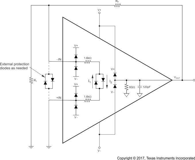
GUID-1FC0714E-C2F5-4C87-86E1-00C12906C588-low.gif Figure 7-7 OPA564-Q1: Output Shutdown Equivalent Circuit (With External Feedback)