SBOS567A June   2011  – February 2024 OPA564-Q1

PRODUCTION DATA  

  1.   1
  2. Features
  3. Applications
  4. Description
  5. Device Comparison Table
  6. Pin Configuration and Functions
  7. Specifications
    1. 6.1 Absolute Maximum Ratings
    2. 6.2 ESD Ratings
    3. 6.3 Recommended Operating Conditions
    4. 6.4 Thermal Information
    5. 6.5 Electrical Characteristics
    6. 6.6 Typical Characteristics
  8. Detailed Description
    1. 7.1 Overview
    2. 7.2 Functional Block Diagram
    3. 7.3 Feature Description
      1. 7.3.1 Adjustable Current Limit
        1. 7.3.1.1 Setting the Current Limit
      2. 7.3.2 Enable and Shutdown (E/S) Pin
      3. 7.3.3 Input Protection
      4. 7.3.4 Output Shutdown
      5. 7.3.5 Microcontroller Compatibility
      6. 7.3.6 Current Limit Flag
      7. 7.3.7 Thermal Protection
      8. 7.3.8 Junction Temperature Measurement Using TSENSE
    4. 7.4 Device Functional Modes
  9. Application and Implementation
    1. 8.1 Application Information
      1. 8.1.1 Basic Configuration
      2. 8.1.2 Output-Stage Compensation
      3. 8.1.3 Output Protection
      4. 8.1.4 Power Dissipation and Safe Operating Area
    2. 8.2 Typical Applications
      1. 8.2.1 Improved Howland Current Pump
      2. 8.2.2 Programmable Power Supply
      3. 8.2.3 Powerline Communication
      4. 8.2.4 Motor-Drive Circuit
      5. 8.2.5 DC Motor-Speed Controller (Without Tachometer)
      6. 8.2.6 Generating VDIG
      7. 8.2.7 Temperature Measurement
    3. 8.3 Power Supply Recommendations
    4. 8.4 Layout
      1. 8.4.1 Layout Guidelines
        1. 8.4.1.1 Thermally Enhanced PowerPAD™ Integrated Circuit Package
          1. 8.4.1.1.1 Bottom-Side Thermal Pad Assembly Process
  10. Device and Documentation Support
    1. 9.1 Receiving Notification of Documentation Updates
    2. 9.2 Support Resources
    3. 9.3 Trademarks
    4. 9.4 Electrostatic Discharge Caution
    5. 9.5 Glossary
  11. 10Revision History
  12. 11Mechanical, Packaging, and Orderable Information

Package Options

Refer to the PDF data sheet for device specific package drawings

Mechanical Data (Package|Pins)
  • DWP|20
Thermal pad, mechanical data (Package|Pins)
Orderable Information

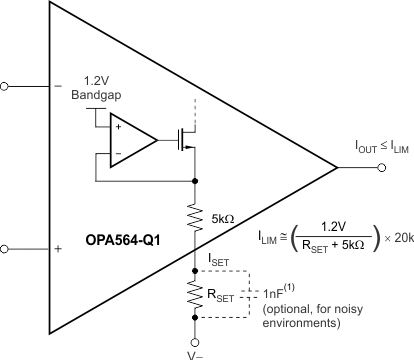
Setting the Current Limit

Leaving the ISET pin unconnected damages the device. Connecting ISET directly to V– is not recommended because direct connection programs the current limit far beyond the 1.5A capability of the device and causes excess power dissipation. The minimum recommended value for RSET is 7.5kΩ, which programs the maximum current limit to approximately 1.9A. The maximum value for RSET is 55kΩ, which programs the minimum current limit to approximately 0.4A. The simplest method for adjusting the current limit (ILIM) uses a resistor or potentiometer connected between the ISET pin and V–, according to Equation 1.

If ILIM has been defined, solve for RSET by rearranging Equation 1 into Equation 3:

Equation 3. R S E T 24 k Ω I L I M - 5 k Ω

RSET in combination with a 5kΩ internal resistor determines the magnitude of a small current that sets the desired output current limit.

Figure 7-1 shows a simplified schematic of the OPA564-Q1 current limit architecture.
GUID-20231219-SS0I-196F-DM0Q-MR7PRCD4F9F4-low.gif
1. At power-on, this capacitor is not charged. Therefore, the OPA564-Q1 is programmed for maximum output current. Capacitor values > 1nF are not recommended.
Figure 7-1 Adjustable Current Limit