SBVS199C June 2012 – January 2024 TLC59283
PRODUCTION DATA
- 1
- 1 Features
- 2 Applications
- 3 Description
- 4 Pin Configurations
- 5 Specifications
- 6 Parameter Measurement Information
- 7 Detailed Description
- 8 Register Configuration
- 9 Application and Implementation
- 10Device and Documentation Support
- 11Revision History
- 12Mechanical, Packaging, and Orderable Information
Package Options
Mechanical Data (Package|Pins)
Thermal pad, mechanical data (Package|Pins)
Orderable Information
5.6 Electrical Characteristics
All minimum and maximum specifications are at TA = –40°C to +85°C and
VCC = 3V to 5.5V, unless otherwise noted.
Typical specifications are at TA = +25°C and VCC = 3.3V.
Typical specifications are at TA = +25°C and VCC = 3.3V.
| PARAMETER | TEST CONDITIONS | TLC59283 | UNIT | |||||
|---|---|---|---|---|---|---|---|---|
| MIN | TYP | MAX | ||||||
| VOH | Output voltage | High | IOH = –2mA at SOUT | VCC – 0.4 | VCC | V | ||
| VOL | Low | IOL = 2mA at SOUT | 0.4 | V | ||||
| VPCHG | Pre-charged voltage | IO = –10µA | VCC – 2.0 | VCC – 1.4 | VCC – 0.8 | V | ||
| VIREF | Reference voltage output | RIREF = 1.5kΩ, TA = +25°C | 1.208 | V | ||||
| IIN | Input current | VIN = VCC or GND at SIN and SCLK | –1 | 1 | μA | |||
| ICC0 | Supply current (VCC) | SIN, SCLK, LAT = GND, BLANK = VOUTn = VCC, RIREF = open | 1 | 2 | mA | |||
| ICC1 | SIN, SCLK, LAT = GND, BLANK =
VOUTn = VCC, RIREF = 3kΩ (IOUT = 17.6mA target) | 3 | 4 | mA | ||||
| ICC2 | All OUTn = ON, SIN,
SCLK, LAT, BLANK = GND, VOUTn = 0.8V, RIREF = 3kΩ | 7 | 9 | mA | ||||
| ICC3 | All OUTn = ON, SIN,
SCLK, LAT, BLANK = GND, VOUTn = 0.8V, RIREF = 1.5kΩ (IOUT = 35.3mA target) | 8 | 11 | mA | ||||
| IOLC | Constant output current | All OUTn = ON,
VOUTn = VOUTfix = 0.8V, RIREF =
1.5kΩ, TA = +25°C (see Figure 6-8) | 32.9 | 35.3 | 37.7 | mA | ||
| IOLKG0 | Output leakage current | All OUTn = OFF, VOUTn = VOUTfix = 10 V, BLANK = VCC, RIREF = 1.5 kΩ (see Figure 6-8) | TJ = +25°C | 0.1 | μA | |||
| TJ = +85°C | 0.2 | μA | ||||||
| TJ = +125°C | 0.07 | 0.5 | μA | |||||
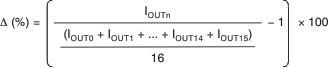
| ΔIOLC0 | Constant-current error | Channel-to-channel(1) | All OUTn = ON,
VOUTn = VOUTfix = 0.8V, RIREF =
1.5kΩ, TA = +25°C (see Figure 6-8) | ±1.4 | ±3 | % | ||
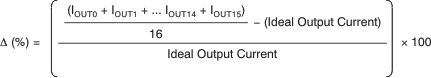
| ΔIOLC1 | Device-to-device(2) | All OUTn = ON,
VOUTn = VOUTfix = 0.8V, RIREF =
1.5kΩ, TA = +25°C (see Figure 6-8) | ±2 | ±4 | % | |||
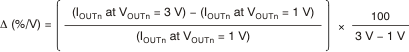
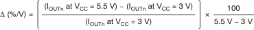
| ΔIOLC2 | Line regulation(3) | All OUTn = ON,
VOUTn = VOUTfix = 0.8V, RIREF =
1.5kΩ, VCC = 3V to 5.5V | ±0.05 | ±1 | %/V | |||
| ΔIOLC3 | Load regulation(4) | All OUTn = ON,
VOUTn = 0.8V to 3V, VOUTfix = 0.8V, RIREF = 1.5kΩ | ±0.5 | ±1 | %/V | |||
| RPUP | Resistor | Pull-up | BLANK | 250 | 500 | 750 | kΩ | |
| RPDWN | Pull-down | LAT | 250 | 500 | 750 | kΩ | ||
| RPCHG | Pre-charge FET on-resistance | VCC = 5.0V,
VOUTn = 0V, OUT0 to OUT15, BLANK = VCC, TA = +25°C | 3 | 6 | kΩ | |||
(1) The deviation of each output from the average of OUT0 to OUT15 constant-current. Deviation is calculated by the formula:
(2) The deviation of the OUT0 to OUT15 constant-current average from the ideal constant-current value.
Deviation is calculated by the following formula:
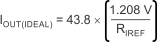
Ideal current is calculated by the formula:
Deviation is calculated by the following formula:
Ideal current is calculated by the formula:
(3) Line regulation is calculated by this equation:
(4) Load regulation is calculated by the equation: