SBVS199C June 2012 – January 2024 TLC59283
PRODUCTION DATA
- 1
- 1 Features
- 2 Applications
- 3 Description
- 4 Pin Configurations
- 5 Specifications
- 6 Parameter Measurement Information
- 7 Detailed Description
- 8 Register Configuration
- 9 Application and Implementation
- 10Device and Documentation Support
- 11Revision History
- 12Mechanical, Packaging, and Orderable Information
Package Options
Mechanical Data (Package|Pins)
Thermal pad, mechanical data (Package|Pins)
Orderable Information
7.3.3.1 Internal Pre-Charge FET
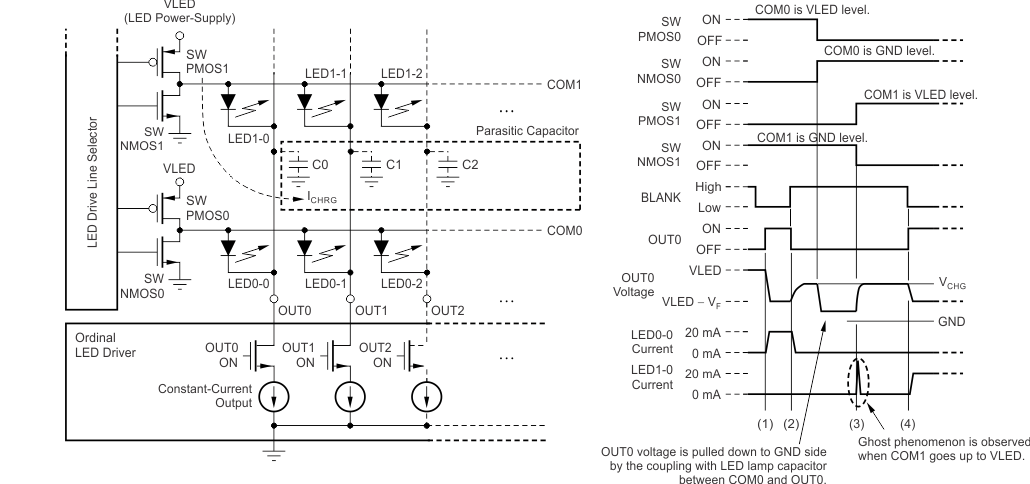
The internal pre-charge FET prevents ghosting of multiplexed LED modules. One cause of this phenomenon is the parasitic capacitance charging current of the constant-current outputs (OUTn) and PCB wiring connected to OUTn through the LED. One of the mechanisms is shown in Figure 7-1.
In Figure 7-1, the constant-current driver turns LED0-0 on at (1) and off at (2). After LED0-0 is turned off, the OUT0 voltage is pulled up to VCHG by LED0-0. This OUT0 node has some parasitic capacitance (such as the constant-current driver output capacitance and the board layout capacitance shown as C0-2). After LED0-0 turns off, SWPMOS0 is turned off, SWNMOS0 is turned on for COM0, and COM0 is pulled down to GND. Because there is a parasitic capacitance between COM0 and OUT0, the OUT0 voltage is also pulled down to GND. Afterwards, SWPMOS1 is turned on for the next common line (COM1). When SWPMOS1 turns on, the OUT0 voltage is pulled up from the ground voltage to VLED – VF. The charge current (ICHRG) flows to the parasitic capacitor (C0) through LED1-0, causing the LED to briefly turn on and creating a ghosting effect of LED1-0.
 Figure 7-1 LED
Ghost-Lighting Phenomenon Mechanism
Figure 7-1 LED
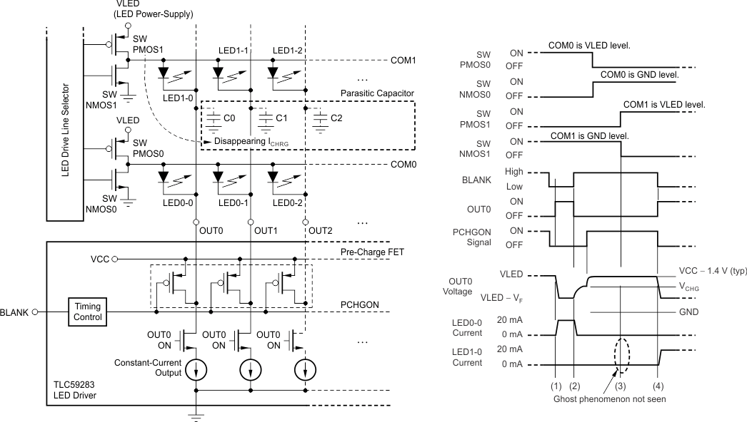
Ghost-Lighting Phenomenon MechanismThe TLC59283 has an internal pre-charge FET to prevent ghosting, as shown in Figure 7-2. When a small delay after PWM control for a single common line completes, the FET pulls OUTn up to VCC. The charge current does not flow to C0 through LED1-0 when SWMOS1 is turned on and the ghosting is eliminated at (3). However, depending on the LED anode voltage, the number of LEDs in series, the LED forward voltage, and the TLC59283 VCC supply voltage, there may not be a great enough ghost-canceling effect.
 Figure 7-2 LED
Ghost-lighting Mechanism by Pre-charge FET