SBVS199C June   2012  – January 2024 TLC59283

PRODUCTION DATA  

  1.   1
  2. Features
  3. Applications
  4. Description
  5. Pin Configurations
  6. Specifications
    1. 5.1 Absolute Maximum Ratings
    2. 5.2 Storage Conditions
    3. 5.3 ESD Ratings
    4. 5.4 Recommended Operating Conditions
    5. 5.5 Thermal Information
    6. 5.6 Electrical Characteristics
    7. 5.7 Timing Characteristics
    8. 5.8 Timing Diagrams
    9. 5.9 Typical Characteristics
  7. Parameter Measurement Information
    1. 6.1 Pin-equivalent Input and Output Schematic Diagrams
    2. 6.2 Test Circuits
  8. Detailed Description
    1. 7.1 Overview
    2. 7.2 Functional Block Diagram
    3. 7.3 Feature Description
      1. 7.3.1 Constant Sink Current Value Setting
      2. 7.3.2 Constant-current Driver On or Off Control
      3. 7.3.3 Noise Reduction
        1. 7.3.3.1 Internal Pre-Charge FET
        2. 7.3.3.2 Improve Output Control Loop Stability
  9. Register Configuration
  10. Application and Implementation
    1. 9.1 Application Information
    2. 9.2 Typical Application
      1. 9.2.1 Design Requirements
      2. 9.2.2 Detailed Design Procedure
      3. 9.2.3 Application Performance Plots
    3. 9.3 Power Supply Recommendations
    4. 9.4 Layout
      1. 9.4.1 Layout Guidelines
      2. 9.4.2 Layout Example
  11. 10Device and Documentation Support
    1. 10.1 Third-Party Products Disclaimer
    2. 10.2 Documentation Support
      1. 10.2.1 Related Documentation
    3. 10.3 Receiving Notification of Documentation Updates
    4. 10.4 Support Resources
    5. 10.5 Trademarks
    6. 10.6 Electrostatic Discharge Caution
    7. 10.7 Glossary
  12. 11Revision History
  13. 12Mechanical, Packaging, and Orderable Information

Package Options

Mechanical Data (Package|Pins)
Thermal pad, mechanical data (Package|Pins)
Orderable Information

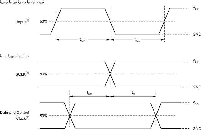
Timing Diagrams

GUID-7BB5BBC5-2DF0-48A0-A7E2-ECE509F37A5D-low.gif
Input pulse rise and fall time is 1ns to 3ns.
Figure 5-1 Input Timing Diagram
GUID-2B8A1567-7076-4524-B3FA-64B14974B366-low.gif
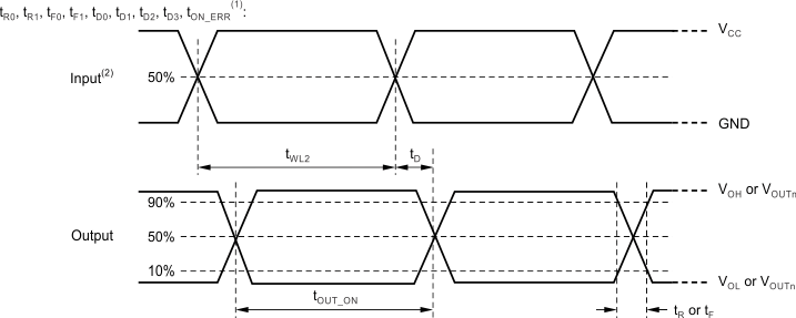
tON_ERR is calculated by tOUTON – tWL2.
Input pulse rise and fall time is 1ns to 3ns.
Figure 5-2 Output Timing Diagram
GUID-F49FD873-ECFE-4B79-B577-2BB4B9743531-low.gif
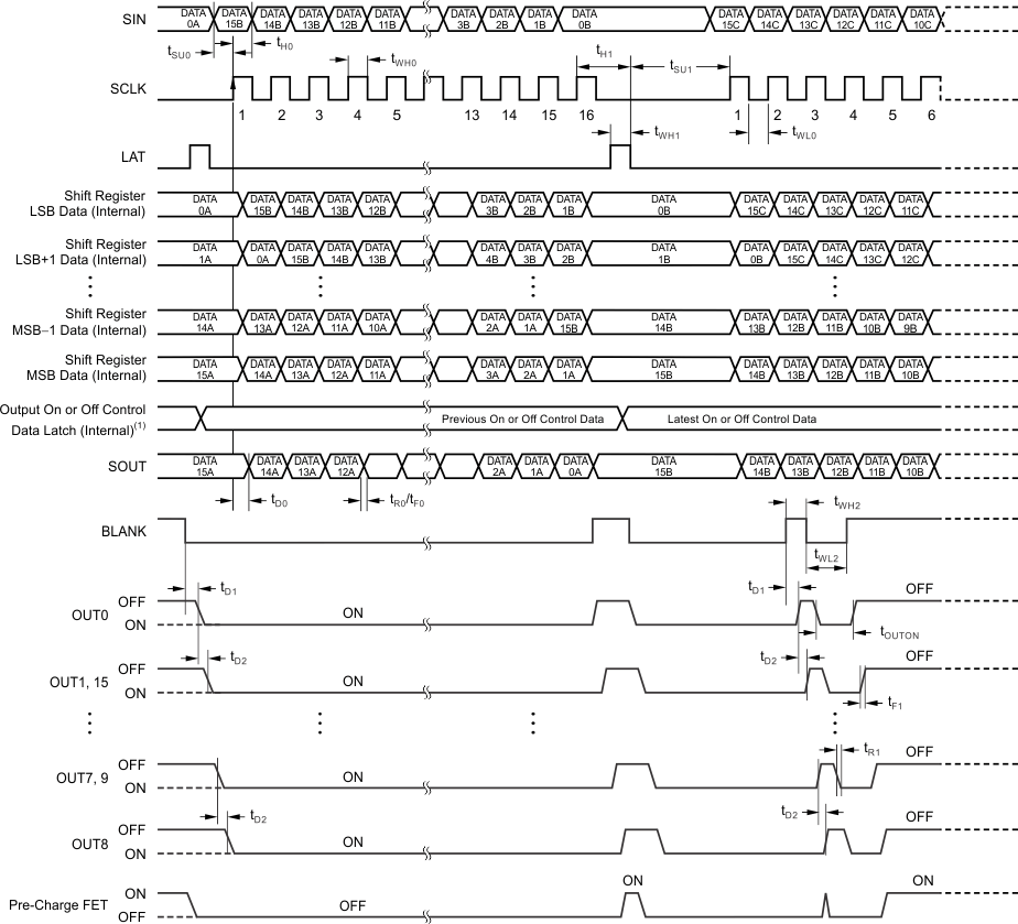
Output on or off data = FFFFh.
tON_ERR = tOUTON – tWL2.
Figure 5-3 Data Write and Output On or Off Timing Diagram