SLUSCK1C July 2016 – June 2018 TPS546C20A
PRODUCTION DATA.
- 1 Features
- 2 Applications
- 3 Description
- 4 Revision History
- 5 Pin Configuration and Functions
- 6 Specifications
-
7 Detailed Description
- 7.1 Overview
- 7.2 Functional Block Diagram
- 7.3
Feature Description
- 7.3.1 2-Phase Application
- 7.3.2 Linear Regulators BP3 and BP6
- 7.3.3 Input Undervoltage Lockout (UVLO)
- 7.3.4 Turnon and Turnoff Delay and Sequencing
- 7.3.5 Voltage Reference
- 7.3.6 Differential Remote Sense and Compensation
- 7.3.7 Set Output Voltage and Adaptive Voltage Scaling (AVS)
- 7.3.8 Reset VOUT
- 7.3.9 Switching Frequency and Synchronization
- 7.3.10 Current Sharing
- 7.3.11 Soft-Start Time and TON_RISE Command
- 7.3.12 Prebiased Output Start-Up
- 7.3.13 Soft-Stop time and TOFF_FALL Command
- 7.3.14 Output Current Telemetry and Low-Side MOSFET Overcurrent Protection
- 7.3.15 High-Side MOSFET Short-Circuit Protection
- 7.3.16 Die Temperature Telemetry and Overtemperature Protection
- 7.3.17 Output Voltage Telemetry and Over-/Under-voltage Protection
- 7.3.18 TON_MAX Fault
- 7.3.19 Power Good (PGOOD) Indicator
- 7.3.20 Fault Protection Responses
- 7.3.21 Switching Node
- 7.3.22 PMBus General Description
- 7.3.23 PMBus Address
- 7.3.24 PMBus Connections
- 7.3.25 Auto ARA (Alert Response Address) Response
- 7.4 Device Functional Modes
- 7.5 Programming
- 7.6
Register Maps
- 7.6.1 OPERATION (01h)
- 7.6.2 ON_OFF_CONFIG (02h)
- 7.6.3 CLEAR_FAULTS (03h)
- 7.6.4 WRITE_PROTECT (10h)
- 7.6.5 STORE_DEFAULT_ALL (11h)
- 7.6.6 RESTORE_DEFAULT_ALL (12h)
- 7.6.7 STORE_USER_ALL (11h)
- 7.6.8 RESTORE_USER_ALL (12h)
- 7.6.9 CAPABILITY (19h)
- 7.6.10 SMBALERT_MASK (1Bh)
- 7.6.11 VOUT_MODE (20h)
- 7.6.12 VOUT_COMMAND (21h)
- 7.6.13 VOUT_MAX (24h)
- 7.6.14 VOUT_TRANSITION_RATE (27h)
- 7.6.15 VOUT_SCALE_LOOP (29h)
- 7.6.16 VOUT_MIN (2Bh)
- 7.6.17 VIN_ON (35h)
- 7.6.18 VIN_OFF (36h)
- 7.6.19 IOUT_CAL_OFFSET (39h)
- 7.6.20 VOUT_OV_FAULT_RESPONSE (41h)
- 7.6.21 VOUT_UV_FAULT_RESPONSE (45h)
- 7.6.22 IOUT_OC_FAULT_LIMIT (46h)
- 7.6.23 IOUT_OC_FAULT_RESPONSE (47h)
- 7.6.24 IOUT_OC_WARN_LIMIT (4Ah)
- 7.6.25 OT_FAULT_LIMIT (4Fh)
- 7.6.26 OT_FAULT_RESPONSE (50h)
- 7.6.27 OT_WARN_LIMIT (51h)
- 7.6.28 TON_DELAY (60h)
- 7.6.29 TON_RISE (61h)
- 7.6.30 TON_MAX_FAULT_LIMIT (62h)
- 7.6.31 TON_MAX_FAULT_RESPONSE (63h)
- 7.6.32 TOFF_DELAY (64h)
- 7.6.33 TOFF_FALL (65h)
- 7.6.34 STATUS_BYTE (78h)
- 7.6.35 STATUS_WORD (79h)
- 7.6.36 STATUS_VOUT (7Ah)
- 7.6.37 STATUS_IOUT (7Bh)
- 7.6.38 STATUS_INPUT (7Ch)
- 7.6.39 STATUS_TEMPERATURE (7Dh)
- 7.6.40 STATUS_CML (7Eh)
- 7.6.41 STATUS_MFR_SPECIFIC (80h)
- 7.6.42 READ_VOUT (8Bh)
- 7.6.43 READ_IOUT (8Ch)
- 7.6.44 READ_TEMPERATURE_1 (8Dh)
- 7.6.45 PMBUS_REVISION (98h)
- 7.6.46 IC_DEVICE_ID (ADh)
- 7.6.47 IC_DEVICE_REV (AEh)
- 7.6.48 MFR_SPECIFIC_00 (D0h)
- 7.6.49 VREF_TRIM (MFR_SPECIFIC_04) (D4h)
- 7.6.50 STEP_VREF_MARGIN_HIGH (MFR_SPECIFIC_05) (D5h)
- 7.6.51 STEP_VREF_MARGIN_LOW (MFR_SPECIFIC_06) (D6h)
- 7.6.52 PCT_OV_UV_WRN_FLT_LIMITS (MFR_SPECIFIC_07) (D7h)
- 7.6.53
OPTIONS (MFR_SPECIFIC_21) (E5h)
- 7.6.53.1 DIS_NEGILIM Bit
- 7.6.53.2 EN_RESET_B Bit
- 7.6.53.3 EN_ADC_CNTL Bit
- 7.6.53.4 VSM Bit
- 7.6.53.5 DLO Bit
- 7.6.53.6 AVG_PROG[1:0] Bits
- 7.6.53.7 EN_AUTO_ARA Bit
- 7.6.53.8 READ_VOUT_RANGE[1:0] Bits
- 7.6.53.9 EN_DRV_IV_VSEL Bit
- 7.6.53.10 RST_VOUT_oSD Bit
- 7.6.53.11 DIS_VSEL Bit
- 7.6.53.12 RSMLO_VAL Bit
- 7.6.53.13 RSMHI_VAL Bit
- 7.6.54 MISC_CONFIG_OPTIONS (MFR_SPECIFIC_32) (F0h)
-
8 Application and Implementation
- 8.1 Application Information
- 8.2
Typical Application
- 8.2.1
4.5-V to 18-V Input, 1-V Typical Output, 35-A Converter
- 8.2.1.1 Design Requirements
- 8.2.1.2
Detailed Design Procedure
- 8.2.1.2.1 Custom Design With WEBENCH® Tools
- 8.2.1.2.2 Switching Frequency Selection
- 8.2.1.2.3 Inductor Selection
- 8.2.1.2.4 Output Capacitor Selection
- 8.2.1.2.5 Output Voltage Deviation During Load Transient
- 8.2.1.2.6 Output Voltage Ripple
- 8.2.1.2.7 Input Capacitor Selection
- 8.2.1.2.8 AVIN, BP6, BP3 Bypass Capacitor
- 8.2.1.2.9 Bootstrap Capacitor Selection
- 8.2.1.2.10 R-C Snubber
- 8.2.1.2.11 Output Voltage Setting and Frequency Compensation Selection
- 8.2.1.2.12 Key PMBus Parameter Selection
- 8.2.1.2.13 Enable, UVLO
- 8.2.1.2.14 Soft-Start Time
- 8.2.1.2.15 Overcurrent Threshold and Response
- 8.2.1.3 Application Curves
- 8.2.1
4.5-V to 18-V Input, 1-V Typical Output, 35-A Converter
- 9 Power Supply Recommendations
- 10Layout
- 11Device and Documentation Support
- 12Mechanical, Packaging, and Orderable Information
Package Options
Refer to the PDF data sheet for device specific package drawings
Mechanical Data (Package|Pins)
- RVF|40
Thermal pad, mechanical data (Package|Pins)
- RVF|40
Orderable Information
7.3.9.1.2 Master-Slave Configuration
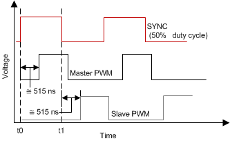
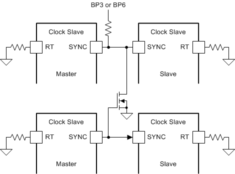
Without the requirement of an external clock, the SYNC pin of the PWM-loop master device can be configured as SYNC-OUT and output a 50% duty-cycle clock to the slave device. The slave device is then synchronized to the falling edge of the clock applied to the SYNC pin. Both the loop master and slave devices require an RT resistor to set the free-running frequency. Figure 27 shows the simplified schematic for this configuration. For the loop slave device in a 2-phase configuration, the SYNC pin is always configured as SYNC-IN, and is synchronized to the falling edge of the incoming clock on the SYNC pin. Figure 28 shows the timing for phase interleaving.
 Figure 27. Master-Slave Synchronization and Phase Interleaving Setting
 Figure 28. Phase Interleaving Timing
An external clock can optionally be applied to both the PWM-loop master and the slave device to synchronize the stack. Only 50% duty cycle of the external clock can be applied to the 2-phase stack to realize the interleaving of two phases. The loop master automatically (auto) detects if an external clock is available for synchronisation. One clock master can also sync another stack as shown in Figure 29. When the auto detection determines the clock master and clock slave, the configuration cannot change until AVIN power cycling.
The EEPROM setup (FORCE_SYNC_IN Bit and FORCE_SYNC_OUT Bit) overrides auto detection of the SYNC pin. Therefore, if the FORCE_SYNC_OUT Bit is set to 1, the user should not apply the external clock to SYNC pin, which may cause catastrophic damage to the device. The FORCE_SYNC_IN Bit has higher priority than the FORCE_SYNC_OUT Bit. Neither the FORCE_SYNC_IN Bit nor the FORCE_SYNC_OUT Bit are set as a factory-default setting.
 Figure 29. Phase Interleaving Timing