SNLS346C August 2011 – June 2014 DS90UR903Q-Q1 , DS90UR904Q-Q1
PRODUCTION DATA.
- 1 Features
- 2 Applications
- 3 Description
- 4 Revision History
- 5 Pin Configuration and Functions
-
6 Specifications
- 6.1 Absolute Maximum Ratings
- 6.2 Handling Ratings
- 6.3 Recommended Operating Conditions
- 6.4 Thermal Information
- 6.5 Electrical Characteristics
- 6.6 Recommended Serializer Timing for PCLK
- 6.7 Serial Control Bus AC Timing Specifications (SCL, SDA) - I2C Compliant (See )
- 6.8 Serial Control Bus DC Characteristics (SCL, SDA) - I2C Compliant
- 6.9 Serializer Switching Characteristics
- 6.10 Deserializer Switching Characteristics
- 6.11 Typical Characteristics
- 7 Detailed Description
- 8 Application and Implementation
- 9 Power Supply Recommendations
- 10Layout
- 11Device and Documentation Support
- 12Mechanical, Packaging, and Orderable Information
Package Options
Mechanical Data (Package|Pins)
- RHS|48
Thermal pad, mechanical data (Package|Pins)
- RHS|48
Orderable Information
1 Features
- 10 MHz to 43 MHz Input PCLK Support
- 210 Mbps to 903 Mbps Data Throughput
- Single Differential Pair Interconnect
- Embedded Clock with DC Balanced Coding to Support AC-coupled Interconnects
- Capable to Drive up to 10 meters Shielded Twisted-Pair
- I2C Compatible Serial Interface for Device Configuration
- Single Hardware Device Addressing Pin
- LOCK Output Reporting Pin to Validate Link Integrity
- Integrated Termination Resistors
- 1.8V- or 3.3V-compatible Parallel Bus Interface
- Single Power Supply at 1.8V
- ISO 10605 ESD and IEC 61000-4-2 ESD Compliant
- Automotive Grade Product: AEC-Q100 Grade 2 Qualified
- Temperature Range −40°C to +105°C
- No Reference Clock Required on Deserializer
- Programmable Receive Equalization
- EMI/EMC Mitigation
- DES Programmable Spread Spectrum (SSCG) outputs
- DES Receiver Staggered Outputs
2 Applications
- Automotive Display Systems
- Central Information Displays
- Navigation Displays
- Rear Seat Entertainment
3 Description
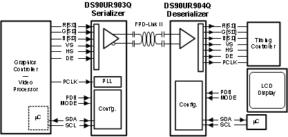
The DS90UR903Q/DS90UR904Q chipset offers a FPD-Link II interface with a high-speed forward channel for data transmission over a single differential pair. The Serializer/ Deserializer pair is targeted for direct connections between graphics host controller and displays modules. This chipset is ideally suited for driving video data to displays requiring 18-bit color depth (RGB666 + HS, VS, and DE). The serializer converts 21 bit data over a single high-speed serial stream. This single serial stream simplifies transferring a wide data bus over PCB traces and cable by eliminating the skew problems between parallel data and clock paths. This significantly saves system cost by narrowing data paths that in turn reduce PCB layers, cable width, and connector size and pins.
The Deserializer inputs provide equalization control to compensate for loss from the media over longer distances. Internal DC balanced encoding/decoding is used to support AC-Coupled interconnects.
The Serializer is offered in a 40-pin WQFN package and the Deserializer is offered in a 48-pin WQFN package.
Device Information(1)
| PART NUMBER | PACKAGE | BODY SIZE (NOM) |
|---|---|---|
| DS90UR903Q-Q1 | WQFN RTA (40) | 6.00 mm × 6.00 mm |
| DS90UR904Q-Q1 | WQFN RHS (48) | 7.00 mm × 7.00 mm |
- For all available packages, see the orderable addendum at the end of the datasheet.
Simplified Schematic
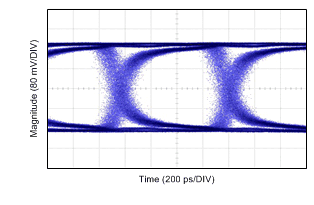
Typical Eye Diagram