JAJSES9 February 2018 DAC8771
PRODUCTION DATA.
- 1 特長
- 2 アプリケーション
- 3 概要
- 4 改訂履歴
- 5 Device Comparison Table
- 6 Pin Configuration and Functions
- 7 Specifications
-
8 Detailed Description
- 8.1 Overview
- 8.2 Functional Block Diagram
- 8.3
Feature Description
- 8.3.1 Current Output Stage
- 8.3.2 Voltage Output Stage
- 8.3.3 Buck-Boost Converter
- 8.3.4 Analog Power Supply
- 8.3.5 Digital Power Supply
- 8.3.6 Internal Reference
- 8.3.7 Power-On-Reset
- 8.3.8 ALARM Pin
- 8.3.9 Power GOOD bit
- 8.3.10 Status Register
- 8.3.11 Status Mask
- 8.3.12 Alarm Action
- 8.3.13 Watchdog Timer
- 8.3.14 Programmable Slew Rate
- 8.3.15 HART Interface
- 8.4 Device Functional Modes
- 8.5
Register Maps
- 8.5.1
Register Maps
- 8.5.1.1 DAC8771 Commands
- 8.5.1.2
Register Maps and Bit Functions
- 8.5.1.2.1 No Operation Register (address = 0x00) [reset = 0x0000]
- 8.5.1.2.2 Reset Register (address = 0x01) [reset = 0x0000]
- 8.5.1.2.3 Reset Config Register (address = 0x02) [reset = 0x0000]
- 8.5.1.2.4 Select DAC Register (address = 0x03) [reset = 0x0000]
- 8.5.1.2.5 Configuration DAC Register (address = 0x04) [reset = 0x0000]
- 8.5.1.2.6 DAC Data Register (address = 0x05) [reset = 0x0000]
- 8.5.1.2.7 Select Buck-Boost Converter Register (address = 0x06) [reset = 0x0000]
- 8.5.1.2.8 Configuration Buck-Boost Register (address = 0x07) [reset = 0x0000]
- 8.5.1.2.9 DAC Channel Calibration Enable Register (address = 0x08) [reset = 0x0000]
- 8.5.1.2.10 DAC Channel Gain Calibration Register (address = 0x09) [reset = 0x0000]
- 8.5.1.2.11 DAC Channel Offset Calibration Register (address = 0x0A) [reset = 0x0000]
- 8.5.1.2.12 Status Register (address = 0x0B) [reset = 0x1000]
- 8.5.1.2.13 Status Mask Register (address = 0x0C) [reset = 0x0000]
- 8.5.1.2.14 Alarm Action Register (address = 0x0D) [reset = 0x0000]
- 8.5.1.2.15 User Alarm Code Register (address = 0x0E) [reset = 0x0000]
- 8.5.1.2.16 Reserved Register (address = 0x0F) [reset = N/A]
- 8.5.1.2.17 Write Watchdog Timer Register (address = 0x10) [reset = 0x0000]
- 8.5.1.2.18 Reserved Register (address 0x12 - 0xFF) [reset = N/A]
- 8.5.1
Register Maps
- 9 Application and Implementation
- 10Power Supply Recommendations
- 11Layout
- 12デバイスおよびドキュメントのサポート
- 13メカニカル、パッケージ、および注文情報
パッケージ・オプション
メカニカル・データ(パッケージ|ピン)
- RGZ|48
サーマルパッド・メカニカル・データ
- RGZ|48
発注情報
9.2.3 Detailed Design Procedure
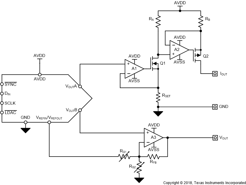
 Figure 126. Generic Design for Typical PLC Current and Voltage Outputs
Figure 126 illustrates a common generic solution for realizing the desired voltage and current output spans for industrial automation applications.
The current output circuit is comprised of amplifiers A1 and A2, MOSFETs Q1 and Q2, and the three resistors RSET, RA, and RB. This two-stage current source enables the ground-referenced DAC output voltage to drive the high-side amplifier required for the current-source.
The voltage output circuit is composed of amplifier A3 and the resistor network consisting of RFB, RG1, and RG2. A3 operates as a modified summing amplifier, where the DAC controls the non-inverting input and inverting input has one path to GND and a second to VREF. This configuration allows the single-ended DAC to create both the unipolar 0-V to 5-V and 0-V to 10-V outputs and the bipolar ±5-V and ±10-V outputs by modifying the values of RG1 and RG2.
Though this generic circuit realizes the desired spans, both the voltage and current outputs have short-comings. The current output high-side supply voltage is typically 24 V, when driving low impedance loads with this supply voltage a considerable amount of power is dissipated on RB and Q2. This power dissipation results in increased heat which leads to drift errors for amplifiers A1 and A2 as well as the DAC, resistors, and the reference voltage. In order to reduce the power dissipation in the high-side voltage to current converter circuit a feedback system which monitors the voltage drop across Q2 and adaptively adjusts the high-side supply voltage can be implemented. This feedback system adjusts the high side supply voltage to the minimum supply required to keep Q2 in the linear region of operation, avoiding compliance voltage saturation, reducing power dissipation and heat to a minimum which helps maintain accuracy.
The generic voltage output circuit performs well but does not compensate for errors associated with excessive output impedance or differences in ground potential from the local PLC ground and the load ground. A modified circuit can be implemented which provides connections to sense errors associated with both output impedance voltage drops and differences in ground potentials, this circuit is shown in Figure 123.
Figure 125 illustrates the DAC8771 along with the LM5160 in a single-channel PLC analog output module. The DAC8771 includes the generic voltage and current output circuits along with buck-boost converter and feedback circuits for the current output and positive and negative sense connections for the voltage output circuit. The DAC8771 also includes an internal reference and internal LDO for supplying the field-side of a digital isolator along with the buck-boost converter generating the single or dual high voltage supplies required for the output circuits, all powered from a single supply.
The DAC8771 buck-boost converter operates at peak efficiency with 12-V input voltage with peak power consumption of approximately 250mW. The LM5160 circuit accepts a wide range of input voltages from just above 12 V to 30 V, providing coverage for most standard PLC supply voltages, and buck-converts this supply voltage to the optimal 12-V supply for the DAC8771. Cumulative power dissipation for the DAC8771 and LM5160 is under 550 mW.
Two ISO7641 devices implement galvanic isolation for all of the digital communication lines, though only a single ISO7641 is required for basic communication with the DAC8771 SPI compatible interface. An output protection circuit is included which is designed to provide immunity to the IEC61000-4 industrial transient and radiation test suite. The protection circuit includes transient voltage suppressor (TVS) diodes, clamp-to-rail steering diodes, and pass elements in the form of resistors and ferrite beads.