JAJSCU3 December 2016 DRV401-Q1
PRODUCTION DATA.
- 1 特長
- 2 アプリケーション
- 3 概要
- 4 改訂履歴
- 5 Pin Configuration and Functions
- 6 Specifications
-
7 Detailed Description
- 7.1 Overview
- 7.2 Functional Block Diagram
- 7.3
Feature Description
- 7.3.1 Magnetic Probe (Sensor) Interface
- 7.3.2 PWM Processing
- 7.3.3 Compensation Driver
- 7.3.4 External Compensation Coil Driver
- 7.3.5 Shunt Sense Amplifier
- 7.3.6 Over-Range Comparator
- 7.3.7 Voltage Reference
- 7.3.8 Demagnetization
- 7.3.9 Power-On and Brownout
- 7.3.10 Error Conditions
- 7.3.11 Protection Recommendations
- 7.4 Device Functional Modes
- 8 Application and Implementation
- 9 Power Supply Recommendations
- 10Layout
- 11デバイスおよびドキュメントのサポート
- 12メカニカル、パッケージ、および注文情報
8 Application and Implementation
NOTE
Information in the following applications sections is not part of the TI component specification, and TI does not warrant its accuracy or completeness. TI’s customers are responsible for determining suitability of components for their purposes. Customers should validate and test their design implementation to confirm system functionality.
8.1 Application Information
8.1.1 Functional Principle of Closed-Loop Current Sensors with Magnetic Probe Using the DRV401-Q1 Device
Closed-loop current sensors measure current over wide frequency ranges, including dc. These types of devices offer a contact-free method and an excellent galvanic isolation performance combined with high resolution, accuracy, and reliability.
At dc and in low-frequency ranges, the magnetic field induced from the current in the primary winding is compensated by a current flowing through a compensation winding. A magnetic field probe, located in the magnetic core loop, detects the magnetic flux. This probe delivers the signal to the amplifier that drives the current through the compensation coil, bringing the magnetic flux back to zero. This compensation current is proportional to the primary current, relative to the winding ratio.
In higher-frequency ranges, the compensation winding acts as the secondary winding in the current transformer, while the H-bridge compensation driver is rolled off and provides low output impedance.
A difference amplifier senses the voltage across a small shunt resistor that is connected to the compensation loop. This difference amplifier generates the output voltage that is referenced to REFIN and is proportional to the primary current. The Functional Block Diagram shows the DRV401-Q1 device used as a compensation current sensor.
8.1.2 Basic Connection
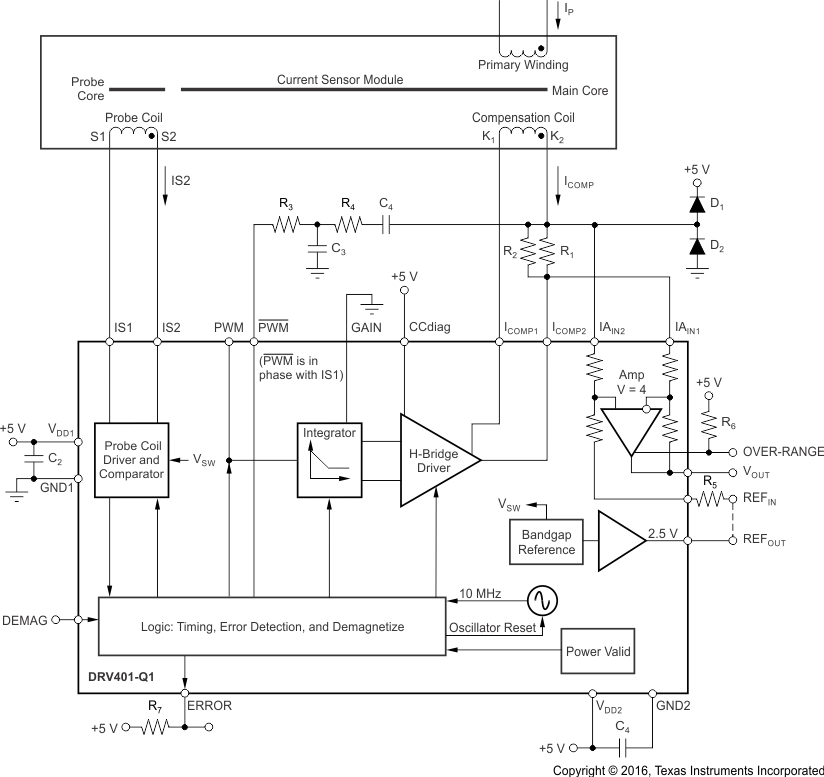
The circuit shown in Figure 42 offers an example of a fully-connected current sensor system.
 Figure 42. Basic Connection Circuit
The connection example in Figure 42 illustrates the few external components required for optimal performance. Each component is described in the following list:
- IP is the primary current to be measured; K1 and K2 connect to the compensation coil. S1 and S2 connect to the magnetic field probe. The dots indicate the winding direction on the sensor main core.
- R1 and R2 form the shunt resistor RSHUNT. This resistance is split into two to allow for adjustments to the required RSHUNT value. The accuracy and temperature stability of these resistors are part of the final system performance.
- R3 and R4, together with C3 and C4, form a network that reduces the remaining probe oscillator ripple in the output signal. The component values depend on the sensor type and are tailored for best results. This network is not required for normal operation.
- R5 is the dummy shunt (RD) resistor used to restore the symmetry of both differential amplifier inputs. R5 = 4 × RSHUNT, but the accuracy is less important.
- R6 and R7 are pull-up resistors connected to the logic outputs.
- C1 and C2 are decoupling capacitors. Use low ESR-type capacitors connected close to the pins. Use low-impedance printed circuit board (PCB) traces, either avoiding vias (plated-through holes) or using multiple vias. A combination of a large (> 1-μF) and a small (< 4.7-nF) capacitor are suggested. When selecting capacitors, make sure to consider the large pulse currents handled from the DRV401-Q1 device.
- D1 and D2 are protection diodes for the differential amplifier input. They are only needed if the voltage drop at RSHUNT exceeds 10 V at the maximum possible peak current.
8.2 Typical Application
The differential (H-bridge) driver arrangement for the compensation coil requires a differential sense amplifier for the shunt voltage. This differential amplifier offers wide bandwidth and a high slew rate for fast current sensors. Excellent dc stability and accuracy result from an auto-zero technique. The voltage gain is 4 V/V, set by precisely matched and stable internal SiCr resistors.
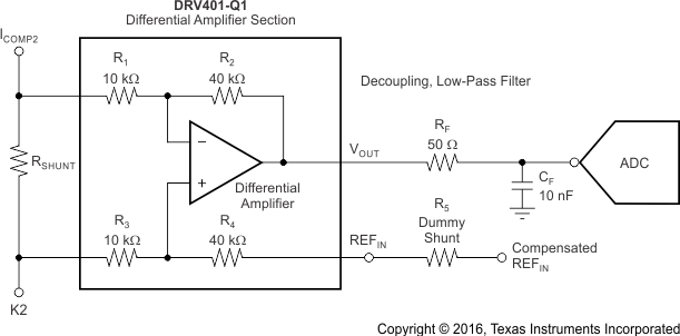
Both inputs of the differential amplifier are normally connected to the current shunt resistor. The resistor adds to the internal (10-kΩ) resistor, slightly reducing the gain in this leg. For best common-mode rejection (CMR), a dummy shunt resistor (R5) is placed in series with the REFIN pin to restore matching of both resistor dividers, as shown in Figure 43.

8.2.1 Design Requirements
- Operate from a single 5-V power supply.
- Measure the compensation coil current with a gain = 4 V/V.
- Maximize the gain accuracy.
- Minimize the common-mode error.
8.2.2 Detailed Design Procedure
For gains of 4 V/V, Equation 2 shows the calculation:

With R2 / R1 = R4 / R3 = 4; R5 = RSHUNT × 4.
Typically, the gain error resulting from the resistance of RSHUNT is negligible; for 70 dB of common-mode rejection, however, the match of both divider ratios must be better than 1/3000.
The amplifier output may drive close to the supply rails, and is designed to drive the input of a successive-approximation resistance (SAR)-type ADC; adding an RC low-pass filter stage between the DRV401-Q1 device and the ADC is recommended. This filter limits the signal bandwidth and decouples the high-frequency component of the converter input sampling noise from the amplifier output. For RF and CF values, see the specific converter recommendations in the specific product data sheet. Empirical evaluation may be necessary to obtain optimum results.
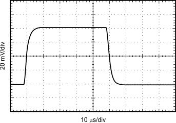
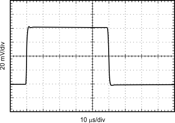
The output drives 100 pF directly and shows 50% overshoot with approximately 1-nF capacitance. Adding RF allows much larger capacitive loads, as shown in Figure 44 and Figure 45.
NOTE
Note that with an RF value of only 20 Ω, the load capacitor must be smaller than 1 nF or larger than 33 nF to avoid overshoot; with an RF value of 50 Ω, this transient area is avoided.
The reference input (REFIN) is the reference node for the exact output signal (VOUT). Connecting REFIN to the reference output (REFOUT) results in a live zero reference voltage of 2.5 V. Using the same reference for REFIN and the ADC avoids mismatch errors that exist between two reference sources.

