JAJSA67I April   2004  – February 2019 LM2743

PRODUCTION DATA.  

  1. 特長
  2. アプリケーション
  3. 概要
    1.     Device Images
      1.      代表的なアプリケーションの図
  4. 改訂履歴
  5. 概要(続き)
  6. Pin Configuration and Functions
    1.     Pin Functions
  7. Specifications
    1. 7.1 Absolute Maximum Ratings
    2. 7.2 ESD Ratings
    3. 7.3 Recommended Operating Conditions
    4. 7.4 Thermal Information
    5. 7.5 Electrical Characteristics
    6. 7.6 Typical Characteristics
  8. Detailed Description
    1. 8.1 Overview
    2. 8.2 Functional Block Diagram
    3. 8.3 Feature Description
      1. 8.3.1  Start Up and Soft-Start
      2. 8.3.2  Normal Operation
      3. 8.3.3  Tracking a Voltage Level
      4. 8.3.4  Tracking Voltage Slew Rate
      5. 8.3.5  Sequencing
      6. 8.3.6  SD Pin Impedance
      7. 8.3.7  MOSFET Gate Drivers
      8. 8.3.8  Power Good Signal
      9. 8.3.9  UVLO
      10. 8.3.10 Current Limit
      11. 8.3.11 Foldback Current Limit
    4. 8.4 Device Functional Modes
      1. 8.4.1 Shutdown
  9. Application and Implementation
    1. 9.1 Application Information
    2. 9.2 Typical Applications
      1. 9.2.1 Synchronous Buck Converter Typical Application using LM2743
        1. 9.2.1.1 Design Requirements
        2. 9.2.1.2 Detailed Design Procedure
          1. 9.2.1.2.1 Custom Design With WEBENCH® Tools
          2. 9.2.1.2.2 Duty Cycle Calculation
          3. 9.2.1.2.3 Input Capacitor
          4. 9.2.1.2.4 Output Inductor
          5. 9.2.1.2.5 Output Capacitor
          6. 9.2.1.2.6 MOSFETs
          7. 9.2.1.2.7 Support Components
          8. 9.2.1.2.8 Control Loop Compensation
          9. 9.2.1.2.9 Efficiency Calculations
        3. 9.2.1.3 Application Curves
      2. 9.2.2 Example Circuit 1
        1. 9.2.2.1 Design Requirements
        2. 9.2.2.2 Detailed Design Procedure
        3. 9.2.2.3 Bill of Materials
      3. 9.2.3 Example Circuit 2
        1. 9.2.3.1 Design Requirements
        2. 9.2.3.2 Detailed Design Procedure
        3. 9.2.3.3 Bill of Materials
      4. 9.2.4 Example Circuit 3
        1. 9.2.4.1 Design Requirements
        2. 9.2.4.2 Detailed Design Procedure
        3. 9.2.4.3 Bill of Materials
  10. 10Power Supply Recommendations
  11. 11Layout
    1. 11.1 Layout Guidelines
    2. 11.2 Layout Example
  12. 12デバイスおよびドキュメントのサポート
    1. 12.1 デバイス・サポート
      1. 12.1.1 開発サポート
        1. 12.1.1.1 WEBENCH®ツールによるカスタム設計
    2. 12.2 ドキュメントの更新通知を受け取る方法
    3. 12.3 コミュニティ・リソース
    4. 12.4 商標
    5. 12.5 静電気放電に関する注意事項
    6. 12.6 Glossary
  13. 13メカニカル、パッケージ、および注文情報

パッケージ・オプション

メカニカル・データ(パッケージ|ピン)
サーマルパッド・メカニカル・データ
発注情報

Sequencing

The start up/soft-start of the LM2743 can be delayed for the purpose of sequencing by connecting a resistor divider from the output of a master power supply to the SD pin, as shown in Figure 22.
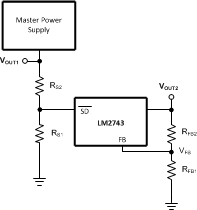
LM2743 20095214.gifFigure 22. Sequencing Circuit

A desired delay time tDELAY between the startup of the master supply output voltage and the LM2743 output voltage can be set based on the SD pin low-to-high threshold VSD-IH and the slew rate of the voltage at the SD pin, SRSD:

Equation 6. tDELAY = VSD-IH / SRSD

Note again, that in Figure 22, the output voltage of the LM2743 has been represented symbolically as VOUT2,. without explicitly showing the power components.

VSD-IH is typically 1.08V and SRSD is the slew rate of the SD pin voltage. The values of the sequencing divider resistors RS1 and RS2 set the SRSD based on the master supply output voltage slew rate, SROUT1, using the following equation:

Equation 7. LM2743 20095287.gif

For example, if the master supply output voltage slew rate was 1V/ms and the desired delay time between the startup of the master supply and LM2743 output voltage was 5ms, then the desired SD pin slew rate would be (1.08V/5 ms) = 0.216 V/ms. Due to the internal impedance of the SD pin, the maximum recommended value for RS2 is 1 kΩ. To achieve the desired slew rate, RS1 would then be 274 Ω. A timing diagram for this example is shown in Figure 23.
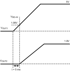
LM2743 20095211.gifFigure 23. Delay for Sequencing