JAJSA67I April   2004  – February 2019 LM2743

PRODUCTION DATA.  

  1. 特長
  2. アプリケーション
  3. 概要
    1.     Device Images
      1.      代表的なアプリケーションの図
  4. 改訂履歴
  5. 概要(続き)
  6. Pin Configuration and Functions
    1.     Pin Functions
  7. Specifications
    1. 7.1 Absolute Maximum Ratings
    2. 7.2 ESD Ratings
    3. 7.3 Recommended Operating Conditions
    4. 7.4 Thermal Information
    5. 7.5 Electrical Characteristics
    6. 7.6 Typical Characteristics
  8. Detailed Description
    1. 8.1 Overview
    2. 8.2 Functional Block Diagram
    3. 8.3 Feature Description
      1. 8.3.1  Start Up and Soft-Start
      2. 8.3.2  Normal Operation
      3. 8.3.3  Tracking a Voltage Level
      4. 8.3.4  Tracking Voltage Slew Rate
      5. 8.3.5  Sequencing
      6. 8.3.6  SD Pin Impedance
      7. 8.3.7  MOSFET Gate Drivers
      8. 8.3.8  Power Good Signal
      9. 8.3.9  UVLO
      10. 8.3.10 Current Limit
      11. 8.3.11 Foldback Current Limit
    4. 8.4 Device Functional Modes
      1. 8.4.1 Shutdown
  9. Application and Implementation
    1. 9.1 Application Information
    2. 9.2 Typical Applications
      1. 9.2.1 Synchronous Buck Converter Typical Application using LM2743
        1. 9.2.1.1 Design Requirements
        2. 9.2.1.2 Detailed Design Procedure
          1. 9.2.1.2.1 Custom Design With WEBENCH® Tools
          2. 9.2.1.2.2 Duty Cycle Calculation
          3. 9.2.1.2.3 Input Capacitor
          4. 9.2.1.2.4 Output Inductor
          5. 9.2.1.2.5 Output Capacitor
          6. 9.2.1.2.6 MOSFETs
          7. 9.2.1.2.7 Support Components
          8. 9.2.1.2.8 Control Loop Compensation
          9. 9.2.1.2.9 Efficiency Calculations
        3. 9.2.1.3 Application Curves
      2. 9.2.2 Example Circuit 1
        1. 9.2.2.1 Design Requirements
        2. 9.2.2.2 Detailed Design Procedure
        3. 9.2.2.3 Bill of Materials
      3. 9.2.3 Example Circuit 2
        1. 9.2.3.1 Design Requirements
        2. 9.2.3.2 Detailed Design Procedure
        3. 9.2.3.3 Bill of Materials
      4. 9.2.4 Example Circuit 3
        1. 9.2.4.1 Design Requirements
        2. 9.2.4.2 Detailed Design Procedure
        3. 9.2.4.3 Bill of Materials
  10. 10Power Supply Recommendations
  11. 11Layout
    1. 11.1 Layout Guidelines
    2. 11.2 Layout Example
  12. 12デバイスおよびドキュメントのサポート
    1. 12.1 デバイス・サポート
      1. 12.1.1 開発サポート
        1. 12.1.1.1 WEBENCH®ツールによるカスタム設計
    2. 12.2 ドキュメントの更新通知を受け取る方法
    3. 12.3 コミュニティ・リソース
    4. 12.4 商標
    5. 12.5 静電気放電に関する注意事項
    6. 12.6 Glossary
  13. 13メカニカル、パッケージ、および注文情報

パッケージ・オプション

メカニカル・データ(パッケージ|ピン)
サーマルパッド・メカニカル・データ
発注情報

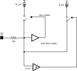
SD Pin Impedance

When connecting a resistor divider to the SD pin of the LM2743 some care has to be taken. Once the SD voltage goes above VSD-IH, a 17-µA pull-up current is activated as shown in Figure 24. This current is used to create the internal hysteresis (≊170 mV); however, high external impedances will affect the SD pin logic thresholds as well. The external impedance used for the sequencing divider network should preferably be a small fraction of the impedance of the SD pin for good performance (around 1 kΩ).
LM2743 20095206.gifFigure 24. SD Pin Logic