JAJSIC9A October   2015  – October 2015 TMP107-Q1

PRODUCTION DATA.  

  1. 特長
  2. アプリケーション
  3. 概要
    1.     Device Images
      1.      代表的なアプリケーション
  4. 改訂履歴
  5. 概要(続き)
  6. Pin Configuration and Functions
    1.     Pin Functions
  7. Specifications
    1. 7.1 Absolute Maximum Ratings
    2. 7.2 ESD Ratings
    3. 7.3 Recommended Operating Conditions
    4. 7.4 Thermal Information
    5. 7.5 Electrical Characteristics
    6. 7.6 Timing Requirements
    7. 7.7 Typical Characteristics
  8. Detailed Description
    1. 8.1 Overview
    2. 8.2 Functional Block Diagram
    3. 8.3 Feature Description
      1. 8.3.1 Digital Temperature Output
      2. 8.3.2 Temperature Limits and Alert
        1. 8.3.2.1 ALERT1, ALERT2, R1, and R2 Pins
      3. 8.3.3 SMAART Wire™ Communication Interface
        1. 8.3.3.1 Communication Protocol
          1. 8.3.3.1.1 Calibration Phase
          2. 8.3.3.1.2 Command and Address Phase
            1. 8.3.3.1.2.1 Global or Individual (G/nI) Bit
            2. 8.3.3.1.2.2 Read/Write (R/nW) Bit
            3. 8.3.3.1.2.3 Command or Address (C/nA) Bit:
          3. 8.3.3.1.3 Register Pointer Phase
          4. 8.3.3.1.4 Data Phase
        2. 8.3.3.2 SMAART Wire™ Operations
          1. 8.3.3.2.1 Command Operations
            1. 8.3.3.2.1.1 Address Initialize
            2. 8.3.3.2.1.2 Last Device Poll
            3. 8.3.3.2.1.3 Global Software Reset
          2. 8.3.3.2.2 Address Operations
            1. 8.3.3.2.2.1 Individual Write
            2. 8.3.3.2.2.2 Individual Read
            3. 8.3.3.2.2.3 Global Write
            4. 8.3.3.2.2.4 Global Read
    4. 8.4 Device Functional Modes
      1. 8.4.1 Continuous-Conversion Mode
      2. 8.4.2 Shutdown Mode
      3. 8.4.3 One-Shot Mode
    5. 8.5 Programming
      1. 8.5.1 EEPROM
      2. 8.5.2 EEPROM Operations
        1. 8.5.2.1 EEPROM Unlock
        2. 8.5.2.2 EEPROM Lock
        3. 8.5.2.3 EEPROM Programming
        4. 8.5.2.4 EEPROM Acquire or Read
    6. 8.6 Register Map
      1. 8.6.1 Temperature Register (address = 0h) [reset = 0h]
        1. Table 4. Temperature Register Field Descriptions
      2. 8.6.2 Configuration Register (address = 1h) [reset = A000h]
        1. Table 5. Configuration Register Field Descriptions
      3. 8.6.3 High Limit 1 Register (address = 2h) [reset = 7FFCh]
        1. Table 7. High Limit 1 Register Field Descriptions
      4. 8.6.4 Low Limit 1 Register (address = 3h) [reset = 8000h]
        1. Table 8. Low Limit 1 Register Field Descriptions
      5. 8.6.5 High Limit 2 Register (address = 4h) [reset = 7FFCh]
        1. Table 9. High Limit 2 Register Field Descriptions
      6. 8.6.6 Low Limit 2 Register (address = 5h) [reset = 8000h]
        1. Table 10. Low Limit 2 Register Field Descriptions
      7. 8.6.7 EEPROM n Register (where n = 1 to 8) (addresses = 6h to Dh) [reset = 0h]
        1. Table 11. EEPROM Register bits
      8. 8.6.8 Die ID Register (address = Fh) [reset = 1107h]
        1. Table 12. Die ID Register Field Descriptions
  9. Application and Implementation
    1. 9.1 Application Information
    2. 9.2 Typical Applications
      1. 9.2.1 Connecting Multiple Devices
        1. 9.2.1.1 Design Requirements
        2. 9.2.1.2 Detailed Design Procedure
          1. 9.2.1.2.1 Voltage Drop Effect
          2. 9.2.1.2.2 EEPROM Programming Current
          3. 9.2.1.2.3 Power Savings
          4. 9.2.1.2.4 Accuracy
          5. 9.2.1.2.5 Electromagnetic Interference (EMI)
        3. 9.2.1.3 Application Curves
      2. 9.2.2 Connecting ALERT1 and ALERT2 Pins
      3. 9.2.3 ALERT1 and ALERT2 Pins Used as General-Purpose Output (GPO)
  10. 10Power Supply Recommendations
  11. 11Layout
    1. 11.1 Layout Guidelines
    2. 11.2 Layout Example
  12. 12デバイスおよびドキュメントのサポート
    1. 12.1 ドキュメントのサポート
      1. 12.1.1 関連資料
    2. 12.2 ドキュメントの更新通知を受け取る方法
    3. 12.3 コミュニティ・リソース
    4. 12.4 商標
    5. 12.5 静電気放電に関する注意事項
    6. 12.6 Glossary
  13. 13メカニカル、パッケージ、および注文情報

パッケージ・オプション

メカニカル・データ(パッケージ|ピン)
サーマルパッド・メカニカル・データ
発注情報

Connecting ALERT1 and ALERT2 Pins

As described in the ALERT1, ALERT2, R1, and R2 Pins section, the TMP107-Q1 contains internal 100-kΩ pullup resistors connected between pins ALERT1 and R1, and pins ALERT2 and R2. Connect R1 and R2 to V+ in order to enable the internal pullup resistors. Figure 42 shows a schematic example of how to connect these pins for multiple TMP107-Q1 devices in a daisy-chain configuration.
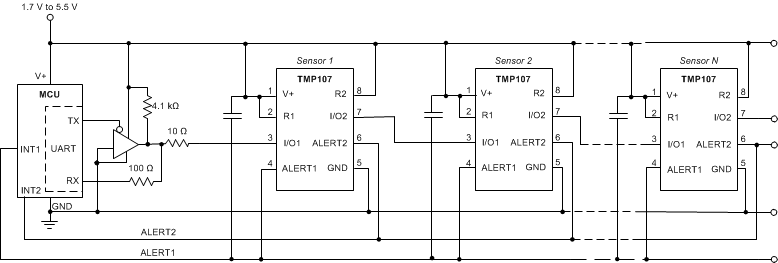
TMP107-Q1 appdiagram3_sbos716.gifFigure 42. Connecting ALERT1 and ALERT2 Pins