JAJSF47A April 2018 – May 2018 UCC28742
PRODUCTION DATA.
- 1 特長
- 2 アプリケーション
- 3 概要
- 4 改訂履歴
- 5 Pin Configuration and Functions
- 6 Specifications
-
7 Detailed Description
- 7.1 Overview
- 7.2 Functional Block Diagram
- 7.3 Feature Description
- 7.4 Device Functional Modes
-
8 Applications and Implementation
- 8.1 Application Information
- 8.2
Typical Application
- 8.2.1 Design Requirements
- 8.2.2
Detailed Design Procedure
- 8.2.2.1 Custom Design With WEBENCH® Tools
- 8.2.2.2 VDD Capacitance, CDD
- 8.2.2.3 VDD Start-Up Resistance, RSTR
- 8.2.2.4 Input Bulk Capacitance and Minimum Bulk Voltage
- 8.2.2.5 Transformer Turns Ratio, Inductance, Primary-Peak Current
- 8.2.2.6 Transformer Parameter Verification
- 8.2.2.7 VS Resistor Divider and Line Compensation
- 8.2.2.8 Standby Power Estimate
- 8.2.2.9 Output Capacitance
- 8.2.2.10 Feedback Loop Design Consideration
- 8.2.3 Application Curves
- 8.3 Do's and Don'ts
- 9 Power Supply Recommendations
- 10Layout
- 11デバイスおよびドキュメントのサポート
- 12メカニカル、パッケージ、および注文情報
10.1 Layout Guidelines
In general, try to keep all high current loop areas as small as possible. Keep all traces with high current and high frequency away from other traces in the design. If necessary, high frequency/high current traces should be perpendicular to signal traces, not parallel to them. Shielding signal traces with ground traces can help reduce noise pick up. Always consider appropriate clearances between the high-voltage connections and any low-voltage nets.
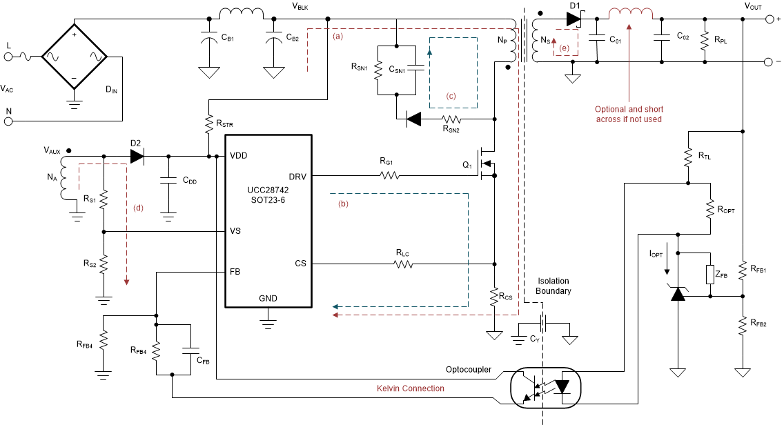
In order to increase the reliability and feasibility of the project it is recommended to adhere to the following guidelines for PCB layout. Figure 25 shows a typical 10-W, 5-V/2-A converter design schematics.
- Minimize stray capacitance on the VS node. Place the voltage sense resistors (RS1 and RS2 in) close to the VS pin.
- Arrange the components to minimize the loop areas of the switching currents as much as possible. These areas include such loops as the transformer primary winding current loop (a), the MOSFET gate-drive loop (b), the primary snubber loop (c), the auxiliary winding loop (d) and the secondary output current loop (e). In practice, trade-offs may have to be made. Loops with higher current should be minimized with higher priority. As a rule of thumb, the priority goes from high to low as (a) – (e) – (c) – (d) – (b).
- The RLC resistor location is critical. To avoid any dv/dt induced noise (for example MOSFET drain dv/dt) coupled onto this resistor, it is better to place RLC closer to the controller and avoid nearby the MOSFET.
- Using Kelvin connection for long distance connection such as for connection between optocoupler and FB pin.
- To improve thermal performance increase the copper area connected to GND pins.
 Figure 25. 10-W, 5-V/2-A Converter Schematics