SBAU378A September 2021 – January 2022 ADS1148 , ADS1248
- Trademarks
- 1Introduction
- 2Getting Started With the ADS1x48EVM
-
3ADS1x48EVM Overview
- 3.1 Analog and Digital Power Supplies
- 3.2 Voltage Reference Options
- 3.3 Clock Options
- 3.4 Digital Interface
- 3.5
Analog Input Connections
- 3.5.1 Connecting a Thermocouple to J5 on the ADS1x48EVM
- 3.5.2 Connecting a Thermistor to J5 on the ADS1x48EVM
- 3.5.3
Connecting an RTD to J6 on the ADS1x48EVM
- 3.5.3.1 Connecting a 2-Wire RTD Using a Low-Side RREF to J6 on the ADS1x48EVM
- 3.5.3.2 Connecting a 2-Wire RTD Using a High-Side RREF to J6 on the ADS1x48EVM
- 3.5.3.3 Connecting a 3-Wire RTD Using One IDAC and a Low-Side RREF to J6 on the ADS1x48EVM
- 3.5.3.4 Connecting a 3-Wire RTD Using One IDAC and a High-Side RREF to J6 on the ADS1x48EVM
- 3.5.3.5 Connecting a 3-Wire RTD Using Two IDACs and a Low-Side RREF to J6 on the ADS1x48EVM
- 3.5.3.6 Connecting a 3-Wire RTD Using Two IDACs and a High-Side RREF to J6 on the ADS1x48EVM
- 3.5.3.7 Connecting a 4-Wire RTD Using a Low-Side RREF to J6 on the ADS1x48EVM
- 3.5.3.8 Connecting a 4-Wire RTD Using a High-Side RREF to J6 on the ADS1x48EVM
- 3.5.3.9 Summary of ADS1x48EVM RTD Configuration Settings
- 3.5.4 Connecting a General-Purpose Input to J5 on the ADS1x48EVM
- 4ADS1x48EVM GUI
- 5Bill of Materials, Printed Circuit Board Layout, and Schematic
- 6Revision History
3.2 Voltage Reference Options
The ADS1x48 is a highly flexible ADC that can accept multiple voltage reference (VREF) options. First, the ADS1x48 integrates a low-noise, 2.048-V reference to help reduce overall component count. Moreover, this internal VREF voltage is supplied externally via the ADS1x48 REFOUT pin and is available on terminal block J5. The ADS1x48 also has two sets of differential VREF inputs defined as REFP0, REFN0 and REFP1, REFN1. All of these options are selected via the MUX1 register in the ADS1x48.
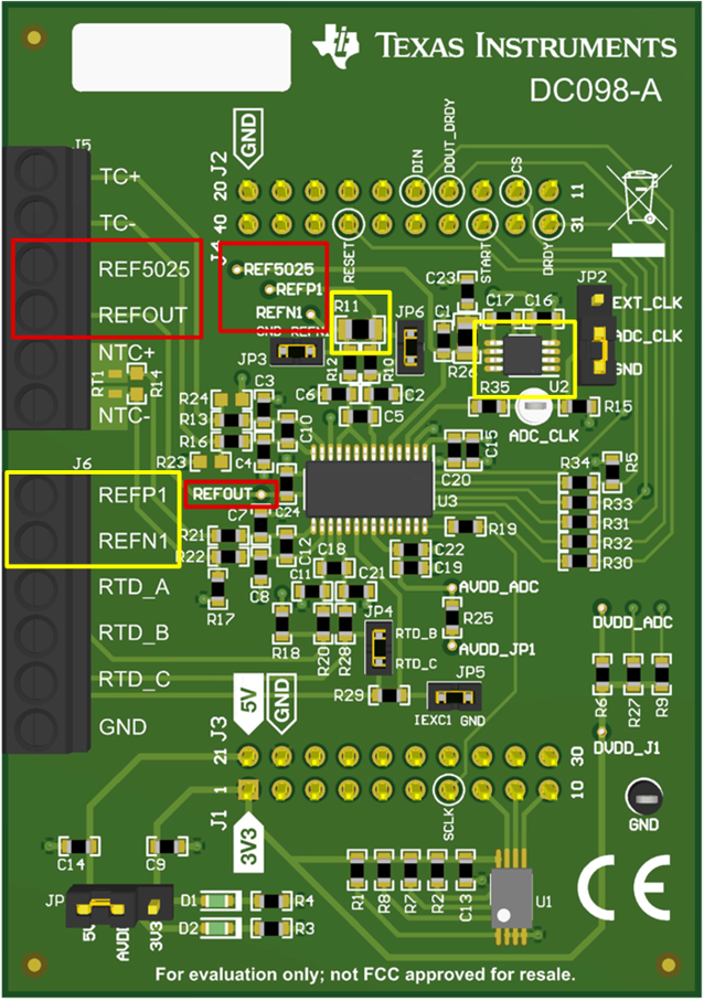
The ADS1x48EVM supports four different VREF options to offer maximum flexibility. Table 3-1 details these four options. Figure 3-3 shows the location of each VREF option (highlighted in yellow) as well as each VREF test point (highlighted in red).
| VREF Mode | VREF Input Channel | Voltage | Location | Test Point | Comment | |
|---|---|---|---|---|---|---|
| Internal | — | 2.048 V | U3 | Output on J5 (REFOUT) | — | |
| External | REF5025 | REFP0, REFN0 | 2.5 V | U2 | Output on J5 (REF5025) | — |
| Ratiometric | REFP1, REFN1 | Variable | R11 | REFP1, REFN1 | Used for RTD measurements | |
| User-provided | REFP1, REFN1 | Variable | J6 (REFP1, REFN1) | REFP1, REFN1 | Remove R11 | |
 Figure 3-3 ADS1x48EVM VREF Options (Yellow) and Test Points (Red)