SBAU378A September 2021 – January 2022 ADS1148 , ADS1248
- Trademarks
- 1Introduction
- 2Getting Started With the ADS1x48EVM
-
3ADS1x48EVM Overview
- 3.1 Analog and Digital Power Supplies
- 3.2 Voltage Reference Options
- 3.3 Clock Options
- 3.4 Digital Interface
- 3.5
Analog Input Connections
- 3.5.1 Connecting a Thermocouple to J5 on the ADS1x48EVM
- 3.5.2 Connecting a Thermistor to J5 on the ADS1x48EVM
- 3.5.3
Connecting an RTD to J6 on the ADS1x48EVM
- 3.5.3.1 Connecting a 2-Wire RTD Using a Low-Side RREF to J6 on the ADS1x48EVM
- 3.5.3.2 Connecting a 2-Wire RTD Using a High-Side RREF to J6 on the ADS1x48EVM
- 3.5.3.3 Connecting a 3-Wire RTD Using One IDAC and a Low-Side RREF to J6 on the ADS1x48EVM
- 3.5.3.4 Connecting a 3-Wire RTD Using One IDAC and a High-Side RREF to J6 on the ADS1x48EVM
- 3.5.3.5 Connecting a 3-Wire RTD Using Two IDACs and a Low-Side RREF to J6 on the ADS1x48EVM
- 3.5.3.6 Connecting a 3-Wire RTD Using Two IDACs and a High-Side RREF to J6 on the ADS1x48EVM
- 3.5.3.7 Connecting a 4-Wire RTD Using a Low-Side RREF to J6 on the ADS1x48EVM
- 3.5.3.8 Connecting a 4-Wire RTD Using a High-Side RREF to J6 on the ADS1x48EVM
- 3.5.3.9 Summary of ADS1x48EVM RTD Configuration Settings
- 3.5.4 Connecting a General-Purpose Input to J5 on the ADS1x48EVM
- 4ADS1x48EVM GUI
- 5Bill of Materials, Printed Circuit Board Layout, and Schematic
- 6Revision History
3.5.3 Connecting an RTD to J6 on the ADS1x48EVM
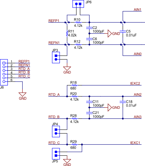
The RTD input connections on J6 are J6:3, J6:4, and J6:5, which correspond to the RTD_A, RTD_B, and RTD_C nets, respectively. Additionally, terminal block J6 provides a pair of differential reference inputs, REFP1 and REFN1, which correspond to inputs J6:1 and J6:2, respectively. The RTD_A, RTD_B and REFP1, REFN1 input pairs have a differential filter with a cutoff frequency of 1.93 kHz. Additionally, each of these inputs has a common-mode filter with a cutoff frequency of 38.63 kHz. Figure 3-12 shows the RTD input structure on the ADS1x48EVM, and Table 3-4 describes the mapping between the terminal block connections, schematic net names, and the analog pins on the ADS1x48. Some nets may connect to multiple analog pins on the ADS1x48.
 Figure 3-12 RTD Input Structure on the ADS1x48EVM
| Connector | Net Name | ADS1x48 Input Connection | Description |
|---|---|---|---|
| J6:1 | REFP1 | REFP1 | External reference input (positive) |
| AIN1 | Analog input 1 | ||
| J6:2 | REFN1 | REFN1 | External reference input (negative) |
| AIN0 | Analog input 0 | ||
| J6:3 | RTD_A | AIN2 | Analog input 2 |
| IEXC2 | Excitation current source #2 | ||
| J6:4 | RTD_B | AIN3 | Analog input 3 |
| IEXC1 | Excitation current source #1 | ||
| J6:5 | RTD_C | IEXC1 | Excitation current source #1 |
| J6:6 | GND | n/a | Analog ground |
In Figure 3-12, resistor R11 is the reference resistor (RREF) that is placed in series with the RTD and connected to the ADS1x48 external reference inputs, as described in Table 3-4. An excitation current supplied by one of the two IDACs integrated into the ADS1x48 flows through RREF and the RTD, creating a ratiometric relationship between the analog input and reference voltages. As a result, the absolute IDAC accuracy is less critical and the system performance improves. However, choose the IDAC current magnitude and the total circuit impedance to ensure that the ADC IDAC compliance voltage is met. For additional information regarding ratiometric references, RTD measurement circuits using precision ADCs, and important specifications including compliance voltage, see the A Basic Guide to RTD Measurements application report.
R11 is chosen to be 4.02 kΩ in order to accommodate high-impedance RTDs at high temperature ranges. For example, a Pt1000 at 850°C has a typical impedance of approximately 3.9 kΩ. If a smaller measurement range is required, replace R11 with a different resistor in an 0805 package or remove R11 and use an external resistor connected between REFP1 and REFN1 on J6. Choose a high accuracy, low-drift resistor to ensure best system performance.
All common RTD configurations can be measured with the ADS1x48EVM, including:
- 2-wire RTD using a low-side RREF
- 2-wire RTD using a high-side RREF
- 3-wire RTD using one IDAC and a low-side RREF
- 3-wire RTD using one IDAC and a high-side RREF
- 3-wire RTD using two IDACs and a low-side RREF
- 3-wire RTD using two IDACs and a high-side RREF
- 4-wire RTD using a low-side RREF
- 4-wire RTD using a high-side RREF
The ADS1x48EVM accomplishes maximum flexibility using jumpers JP3, JP4, JP5, and JP6 (see Figure 3-12) in conjunction with different analog inputs and IDAC routing. The following subsections detail the appropriate connections and settings to enable each RTD configuration using the ADS1x48EVM. Each subsection contains a connection diagram where the red lines indicate how current flows in the circuit. Moreover, the red text indicates which jumpers are populated and which current sources are biasing the RTD, and the blue text indicates the measurement channels. This information is summarized in Section 3.5.3.9.