SBOA418 july 2023 OPA2197-Q1 , OPA392
- 1
- Abstract
- Trademarks
- 1Introduction: Open-Loop Output Impedance (RO)
- 2Overview: Closed-Loop Amplifier Stability
- 3Example, Calculate Optimal Isolation Resistance to Drive Large Load Capacitance
- 4RO, RISO, and Capacitive Load Drive
- 5Derive Equation for Optimal Isolation Resistance
- 6Summary
- 7References
3 Example, Calculate Optimal Isolation Resistance to Drive Large Load Capacitance
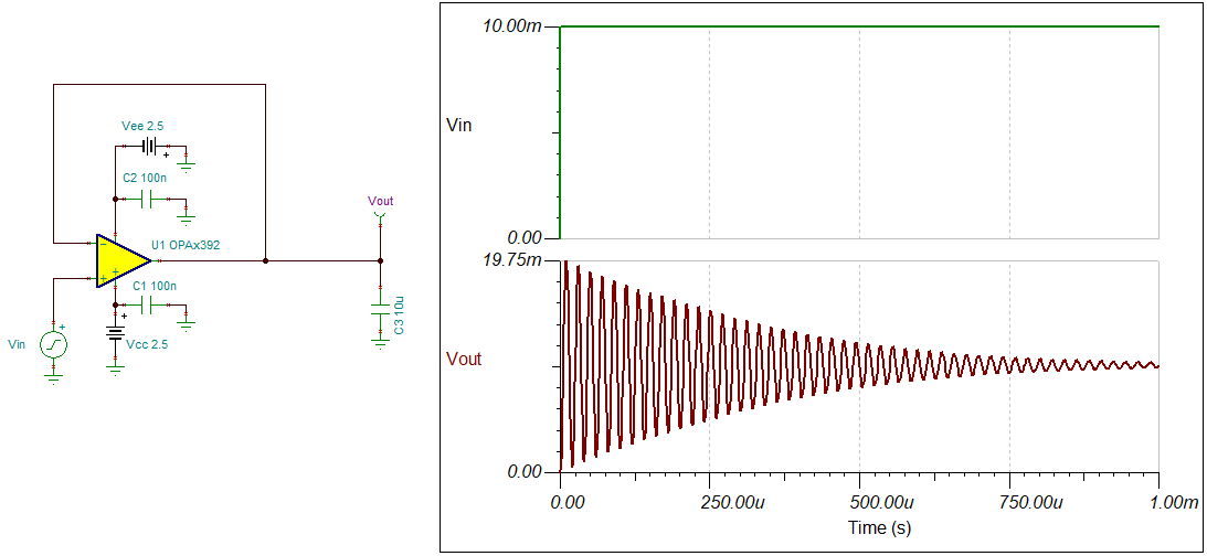
A common case for amplifiers to exhibit instability is when configured to directly drive a large capacitive load. Figure 3-1 shows the OPA392 configured as a buffer with a 10 µF capacitor connected between the output of the amplifier and ground. The 10 µF load causes the circuit to exhibit an undesirable ringing behavior. This ringing behavior indicates that the circuit is unstable. The analysis techniques described in TIPL Video Series on Stability confirm the circuit is unstable with a phase margin of less than 1°.
 Figure 3-1 Unstable Buffer Configuration, 10 µF Load
It is not recommended to directly load an amplifier's output with a large capacitor. However, in certain cases such as an ADC reference driver, this load capacitor is essential to the circuit’s function and the capacitance cannot be removed or reduced. A common technique to stabilize an amplifier driving a capacitive load, is to place a resistor in series between the amplifier’s output and the load capacitance. This is referred to as an isolation resistor or RISO, as it serves to isolate the output and feedback of the amplifier from the capacitive load.
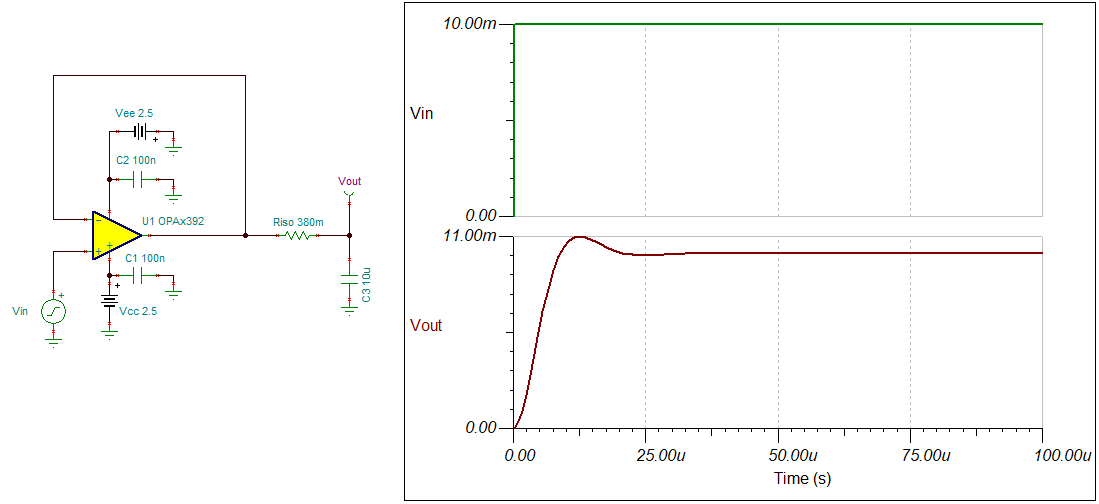
Implementing a small 380 mΩ isolation resistor in the OPA392 buffer circuit improves the phase margin to 60°, and the circuit is stable. Figure 3-2 shows the small-signal step response in which the output settles without oscillations or ringing.
 Figure 3-2 Stable Buffer Configuration with Optimal RISO
The magnitude of the isolation resistance was determined by Equation 2.
Where,
- fgbw is the gain bandwidth of the amplifier in Hz, as defined in the data sheet
- RO is the amplifier’s open-loop output impedance in Ohms, as defined in the data sheet
- CLOAD is the load capacitance in Farads
With the data sheet specifications for gain bandwidth and open-loop output impedance, Equation 2 can be used to quickly determine an optimal isolation resistance to stabilize a circuit driving a large capacitive load. Always use Spice simulation tools such as TINA-TI to verify the circuit is stable and operating with the RISO value chosen.
The relationship between open-loop output impedance, capacitive loading, and closed-loop stability is explored in detail in Section 4. This relationship is then used to derive Equation 2 for optimal RISO when driving a capacitive load.