SBOU180B november   2016  – july 2023 INA260


  1.   1
  2.   INA260EVM-PDK and Software Tutorial
  3.   Trademarks
  4. 1Overview
    1. 1.1 INA260EVM-PDK Contents
    2. 1.2 INA260EVM-PDK Features
    3. 1.3 Related Documentation from Texas Instruments
  5. 2INA260EVM-PDK Hardware
    1. 2.1 SM-USB-DIG Platform Description
    2. 2.2 INA260EVM PCB Description
      1. 2.2.1 EVM Power Supply
      2. 2.2.2 EVM Analog Inputs
    3. 2.3 EVM Digital Inputs and Outputs
  6. 3INA260EVM-PDK (Rev A) Setup
    1. 3.1 One-Time GUI Software Installation
    2. 3.2 INA260EVM Jumper Settings
    3. 3.3 Connecting the Hardware
    4. 3.4 System Power-Up
  7. 4INA260EVM GUI Software
    1. 4.1 Configuration Tool
      1. 4.1.1 Step 1: Set the I2C Address
      2. 4.1.2 Step 2: Configure Operation
      3. 4.1.3 Step 3: Set Conversion Times
      4. 4.1.4 Step 4: Configure Alert
    2. 4.2 Results Bar
    3. 4.3 Graph Tool
    4. 4.4 Registers Tool
  8. 5INA260EVM Documentation
    1. 5.1 Schematic
    2. 5.2 PCB Layout
    3. 5.3 Bill of Materials
  9. 6Revision History

INA260EVM Jumper Settings

Figure 3-3 shows the default jumper configuration for the INA260EVM and Table 3-1 explain the purpose of each jumper. Ensure that the jumpers are installed in the correct positions, based on the required test conditions.
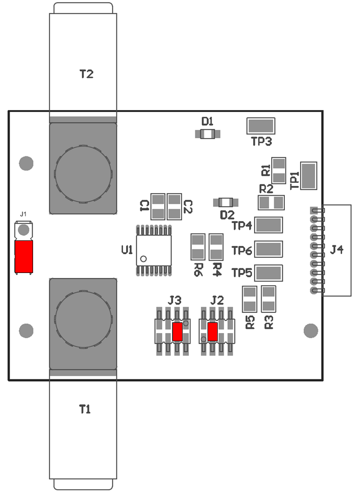
GUID-08834A66-874E-497B-BBA0-AFC4E20E03D9-low.gif Figure 3-3 INA260EVM Default Jumper Settings
Table 3-1 INA260EVM Test Board Jumper Functions

JUMPER

DEFAULT

PURPOSE

J1 IN+ This jumper selects whether the VBUS pin on the INA260 is connected to the IN+ or IN– pin; see Section 2.2.2 for details.
J2 GND This jumper sets the A0 character of the 2-character I2C device address; see Section 2.3 for details.
J3 GND This jumper sets the A1 character of the 2-character I2C device address; see Section 2.3 for details.