SLAU919 November 2023
2.1.2 Jumper Definitions
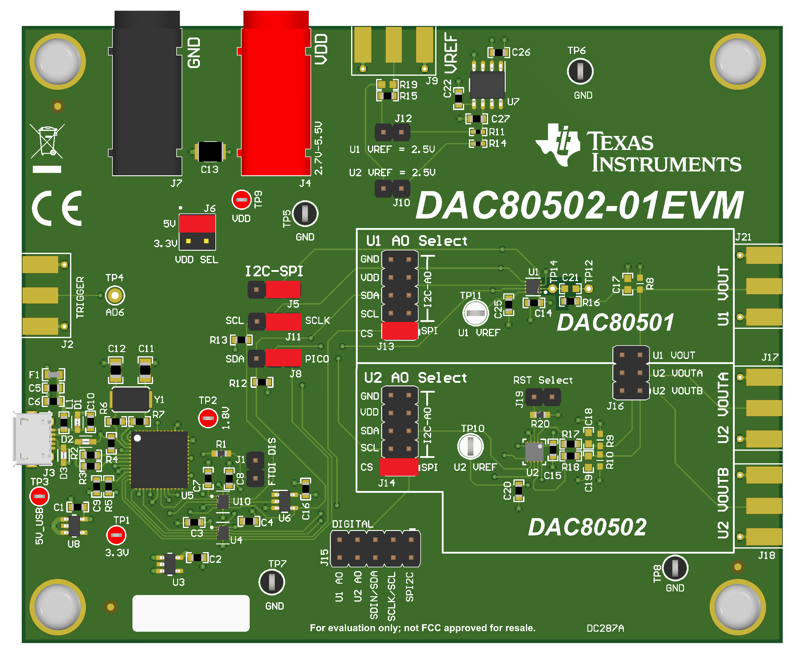
The jumpers must be connected properly to operate the DAC80502-01EVM. Table 3-1 provides the details of the configurable jumper settings of the DAC80502-01EVM. Figure 3-2 shows the default jumper connections on the board.
| Designator | Name | Positions |
|---|---|---|
| J1 | FTDI DIS | SHORT 1-2 – FTDI communication is disabled. OPEN – FTDI communication is enabled (default). |
J5 | I2C-SPI | SHORT 1-2 – SPI2C connected to ground for SPI communication (default). SHORT 2-3 – SPI2C connected to VDD for I2C Configuration. OPEN – SPI2C floating, invalid position. |
J6 | VDD SEL | SHORT 1-2 – VDD is connected to USB 5 V (default). SHORT 3-4 – VDD is connected to on-board 3.3 V. OPEN – VDD is externally powered. |
J8 | SDA - PICO | SHORT 1-2 – Connects the DAC80501 and the DAC80502 SDIN/SDA pins to the FTDI PICO pin for SPI mode (default). SHORT 2-3 – Connects the DAC80501 and the DAC80502 SDIN/SDA pins to the FTDI SDA pin for I2C Mode. OPEN – Open if external communication is used. |
J10 | U2 VREF = 2.5V | SHORT 1-2 – Connects the DAC80502 VREFIO pin to the on-board 2.5-V reference. Make sure the internal reference is powered off before closing this jumper. OPEN – Open if internal reference or external reference via J9 is used (default). If an external reference is used, then turn off the internal reference. |
J11 | SCL - SCLK | SHORT 1-2 – Connects the DAC80501 and the DAC80502 SCLK/SCL pins to the FTDI SCLK pin for SPI mode (default). SHORT 2-3 – Connects the DAC80501 and the DAC80502 SCLK/SCL pins to the FTDI SCL pin for I2C Mode. |
J12 | U1 VREF = 2.5V |
SHORT 1-2 –Connects the DAC80501 VREFIO pin to the on-board 2.5-V reference. Make sure the internal reference is powered off before closing this jumper. OPEN – Open if internal reference or external reference via J9 is used (default). If an external reference is used, then turn off the internal reference. |
J13 | U1 A0 Select | SHORT 1-2 – DAC80501 SPI configuration (default). SHORT all else – DAC80501 I2C configuration, see Table 3-7 for jumper configurations. OPEN – Open if external communication is used. |
J14 | U2 A0 Select | SHORT 1-2 – DAC80502 SPI configuration (default) SHORT all else – DAC80502 I2C configuration, see Table 3-7 for jumper configurations. OPEN – Open if external communication is used. |
J19 | RST Select | SHORT 1-2 – DAC80502 RSTSEL pin is connected to VDD. OPEN – DAC80502 RSTSEL pin is connected to GND (default). |
 Figure 2-2 DAC80502-01EVM Default Jumper Settings