SLVA275C january 2010 – may 2023 UCD9081
- Abstract
- Trademarks
- 1Introduction
- 2Hardware
- 3Software
-
4User Configuration
- 4.1 Configuration Parameter Memory Map
- 4.2
Configuration Parameter Detail
- 4.2.1 GpDir
- 4.2.2 NegateEnablePolarity
- 4.2.3 SeqEventPending
- 4.2.4 SequenceEventParameters
- 4.2.5 SequenceEventLink
- 4.2.6 SequenceEventData
- 4.2.7 DependencyMasks
- 4.2.8 UnderVoltageThresholds
- 4.2.9 OverVoltageThresholds
- 4.2.10 RampTime
- 4.2.11 OutOfRegulationWidth
- 4.2.12 UnsequenceTime
- 4.2.13 EnablePolarity
- 4.2.14 SaveRailLog
- 4.2.15 ReferenceSelect
- 4.2.16 LastUnusedSeq
- 4.2.17 IgnoreGlitchAlarms
- 4.2.18 IgnoreFlashErrorLog
- 4.2.19 Checksum
- 5Additional Considerations
- 6References
- 7Revision History
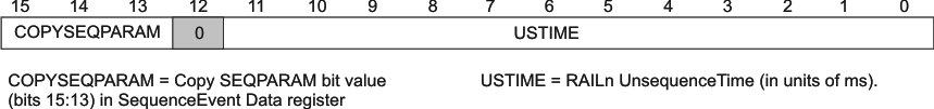
4.2.12 UnsequenceTime
The UnsequenceTime field in the configuration parameters specifies the amount of time that each rail must delay before unsequencing. The address map for these registers is as follows:
| Address | Size | Default Value | Description |
|---|---|---|---|
| 0xE150 | 2 | 0xC0FF | Unsequence delay for rail 1 |
| 0xE152 | 2 | 0xC1FF | Unsequence delay for rail 2 |
| 0xE154 | 2 | 0xC2FF | Unsequence delay for rail 3 |
| 0xE156 | 2 | 0xC3FF | Unsequence delay for rail 4 |
| 0xE158 | 2 | 0xC4FF | Unsequence delay for rail 5 |
| 0xE15A | 2 | 0xC5FF | Unsequence delay for rail 6 |
| 0xE15C | 2 | 0xC6FF | Unsequence delay for rail 7 |
| 0xE15E | 2 | 0xC7FF | Unsequence delay for rail 8 |
| 0xE160 | 2 | 0x0000 | Unsequence delay for GPO1 |
| 0xE162 | 2 | 0xC000 | Unsequence delay for GPO2 |
| 0xE164 | 2 | 0xC000 | Unsequence delay for GPO3 |
| 0xE166 | 2 | 0xC000 | Unsequence delay for GPO4 |
The contents of this register are as follows: