SLVA275C january 2010 – may 2023 UCD9081
- Abstract
- Trademarks
- 1Introduction
- 2Hardware
- 3Software
-
4User Configuration
- 4.1 Configuration Parameter Memory Map
- 4.2
Configuration Parameter Detail
- 4.2.1 GpDir
- 4.2.2 NegateEnablePolarity
- 4.2.3 SeqEventPending
- 4.2.4 SequenceEventParameters
- 4.2.5 SequenceEventLink
- 4.2.6 SequenceEventData
- 4.2.7 DependencyMasks
- 4.2.8 UnderVoltageThresholds
- 4.2.9 OverVoltageThresholds
- 4.2.10 RampTime
- 4.2.11 OutOfRegulationWidth
- 4.2.12 UnsequenceTime
- 4.2.13 EnablePolarity
- 4.2.14 SaveRailLog
- 4.2.15 ReferenceSelect
- 4.2.16 LastUnusedSeq
- 4.2.17 IgnoreGlitchAlarms
- 4.2.18 IgnoreFlashErrorLog
- 4.2.19 Checksum
- 5Additional Considerations
- 6References
- 7Revision History
4.2.8 UnderVoltageThresholds
The UnderVoltageThresholds field in the configuration parameters specifies each rail undervoltage threshold that is used when monitoring this rail. The address map for these registers is as follows:
| Address | Size | Default Value | Description |
|---|---|---|---|
| 0xE110 | 2 | 0x0000 | Undervoltage threshold for rail 8 |
| 0xE112 | 2 | 0x0000 | Undervoltage threshold for rail 7 |
| 0xE114 | 2 | 0x0000 | Undervoltage threshold for rail 6 |
| 0xE116 | 2 | 0x0000 | Undervoltage threshold for rail 5 |
| 0xE118 | 2 | 0x0000 | Undervoltage threshold for rail 4 |
| 0xE11A | 2 | 0x0000 | Undervoltage threshold for rail 3 |
| 0xE11C | 2 | 0x0000 | Undervoltage threshold for rail 2 |
| 0xE11E | 2 | 0x0000 | Undervoltage threshold for rail 1 |
The format for each register is as follows:

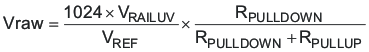
The voltage conversion depends on the configured voltage reference, and the pullup/pulldown resistors used on the board for each rail. The voltage reference is selected as either 2.5 V (internal) or VCC (external). The formula to convert the desired rail UnderVoltageThreshold to Vraw follows:
Without external rail voltage divider:
Equation 1. 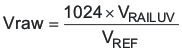
With external rail voltage divider:
Equation 2.